Diode


In electronics, a diode is a two-terminal electronic component that conducts primarily in one direction (asymmetric conductance); it has low (ideally zero) resistance to the flow of current in one direction, and high (ideally infinite) resistance in the other. A semiconductor diode, the most common type today, is a crystalline piece of semiconductor material with a p–n junction connected to two electrical terminals.[5] A vacuum tube diode has two electrodes, a plate (anode) and a heated cathode. Semiconductor diodes were the first semiconductor electronic devices. The discovery of crystals' rectifying abilities was made by German physicist Ferdinand Braun in 1874. The first semiconductor diodes, called cat's whisker diodes, developed around 1906, were made of mineral crystals such as galena. Today, most diodes are made of silicon, but other semiconductors such as selenium or germanium are sometimes used.[6]
Main functions
The most common function of a diode is to allow an electric current to pass in one direction (called the diode's forward direction), while blocking current in the opposite direction (the reverse direction). Thus, the diode can be viewed as an electronic version of a check valve. This unidirectional behavior is called rectification, and is used to convert alternating current (AC) to direct current (DC), including extraction of modulation from radio signals in radio receivers—these diodes are forms of rectifiers.
However, diodes can have more complicated behavior than this simple on–off action, because of their nonlinear current-voltage characteristics. Semiconductor diodes begin conducting electricity only if a certain threshold voltage or cut-in voltage is present in the forward direction (a state in which the diode is said to be forward-biased). The voltage drop across a forward-biased diode varies only a little with the current, and is a function of temperature; this effect can be used as a temperature sensor or as a voltage reference.
A semiconductor diode's current–voltage characteristic can be tailored by selecting the semiconductor materials and the doping impurities introduced into the materials during manufacture. These techniques are used to create special-purpose diodes that perform many different functions. For example, diodes are used to regulate voltage (Zener diodes), to protect circuits from high voltage surges (avalanche diodes), to electronically tune radio and TV receivers (varactor diodes), to generate radio-frequency oscillations (tunnel diodes, Gunn diodes, IMPATT diodes), and to produce light (light-emitting diodes). Tunnel, Gunn and IMPATT diodes exhibit negative resistance, which is useful in microwave and switching circuits.
Diodes, both vacuum and semiconductor, can be used as shot-noise generators.
History
Thermionic (vacuum tube) diodes and solid state (semiconductor) diodes were developed separately, at approximately the same time, in the early 1900s, as radio receiver detectors. Until the 1950s vacuum tube diodes were used more frequently in radios because the early point-contact type semiconductor diodes were less stable. In addition, most receiving sets had vacuum tubes for amplification that could easily have the thermionic diodes included in the tube (for example the 12SQ7 double diode triode), and vacuum tube rectifiers and gas-filled rectifiers were capable of handling some high voltage/high current rectification tasks better than the semiconductor diodes (such as selenium rectifiers) which were available at that time.
Vacuum tube diodes
In 1873, Frederick Guthrie discovered the basic principle of operation of thermionic diodes.[7][8] Guthrie discovered that a positively charged electroscope could be discharged by bringing a grounded piece of white-hot metal close to it (but not actually touching it). The same did not apply to a negatively charged electroscope, indicating that the current flow was only possible in one direction.
Thomas Edison independently rediscovered the principle on February 13, 1880. At the time, Edison was investigating why the filaments of his carbon-filament light bulbs nearly always burned out at the positive-connected end. He had a special bulb made with a metal plate sealed into the glass envelope. Using this device, he confirmed that an invisible current flowed from the glowing filament through the vacuum to the metal plate, but only when the plate was connected to the positive supply.
Edison devised a circuit where his modified light bulb effectively replaced the resistor in a DC voltmeter. Edison was awarded a patent for this invention in 1884.[9] Since there was no apparent practical use for such a device at the time, the patent application was most likely simply a precaution in case someone else did find a use for the so-called Edison effect.
About 20 years later, John Ambrose Fleming (scientific adviser to the Marconi Company and former Edison employee) realized that the Edison effect could be used as a precision radio detector. Fleming patented the first true thermionic diode, the Fleming valve, in Britain on November 16, 1904[10] (followed by U.S. Patent 803,684 in November 1905).
Solid-state diodes
In 1874 German scientist Karl Ferdinand Braun discovered the "unilateral conduction" of crystals.[11][12] Braun patented the crystal rectifier in 1899.[13] Copper oxide and selenium rectifiers were developed for power applications in the 1930s.
Indian scientist Jagadish Chandra Bose was the first to use a crystal for detecting radio waves in 1894.[14] The crystal detector was developed into a practical device for wireless telegraphy by Greenleaf Whittier Pickard, who invented a silicon crystal detector in 1903 and received a patent for it on November 20, 1906.[15] Other experimenters tried a variety of other substances, of which the most widely used was the mineral galena (lead sulfide). Other substances offered slightly better performance, but galena was most widely used because it had the advantage of being cheap and easy to obtain. The crystal detector in these early crystal radio sets consisted of an adjustable wire point-contact, often made of gold or platinum because of their incorrodible nature (the so-called "cat's whisker"), which could be manually moved over the face of the crystal in search of a portion of that mineral with rectifying qualties. This troublesome device was superseded by thermionic diodes (vacuum tubes) by the 1920s, but after high purity semiconductor materials became available, the crystal detector returned to dominant use with the advent, in the 1950s, of inexpensive fixed-germanium diodes. Bell Labs also developed a germanium diode for microwave reception, and AT&T used these in their microwave towers that criss-crossed the nation starting in the late 1940s, carrying telephone and network television signals. Bell Labs did not develop a satisfactory thermionic diode for microwave reception.
Etymology
At the time of their invention, such devices were known as rectifiers. In 1919, the year tetrodes were invented, William Henry Eccles coined the term diode from the Greek roots di (from δί), meaning 'two', and ode (from ὁδός), meaning 'path'. (However, the word diode itself, as well as triode, tetrode, pentode, hexode, were already in use as terms of multiplex telegraphy; see, for example, The telegraphic journal and electrical review, September 10, 1886, p. 252).
Rectifiers
Although all diodes rectify, the term 'rectifier' is normally reserved for higher currents and voltages than would normally be found in the rectification of lower power signals; examples include:
- Power supply rectifiers (half-wave, full-wave, bridge)
- Flyback diodes
World's smallest diode
Researchers from the University of Georgia and Ben-Gurion University of the Negev (BGU) have developed a diode made from a molecule of DNA. Professor Bingqian Xu from the College of Engineering at the University of Georgia and his team took a single DNA molecule made from 11 base pairs and connected it to an electronic circuit a few nanometers in size. When layers of coralyne were inserted between layers of DNA, the current jumped up to 15 times larger negative versus positive, which is necessary for a nano diode.[16][17]
Thermionic diodes


A thermionic diode is a thermionic-valve device (also known as a vacuum tube, tube, or valve), consisting of a sealed evacuated glass envelope containing two electrodes: a cathode heated by a filament, and a plate (anode). Early examples were fairly similar in appearance to incandescent light bulbs.
In operation, a separate current through the filament (heater), a high resistance wire made of nichrome, heats the cathode red hot (800–1000 °C), causing it to release electrons into the vacuum, a process called thermionic emission. The cathode is coated with oxides of alkaline earth metals such as barium and strontium oxides, which have a low work function, to increase the number of electrons emitted. (Some valves use direct heating, in which a tungsten filament acts as both heater and cathode.) The alternating voltage to be rectified is applied between the cathode and the concentric plate electrode. When the plate has a positive voltage with respect to the cathode, it electrostatically attracts the electrons from the cathode, so a current of electrons flows through the tube from cathode to plate. However, when the polarity is reversed and the plate has a negative voltage, no current flows, because the cathode electrons are not attracted to it. The unheated plate does not emit any electrons itself. So electrons can only flow through the tube in one direction, from the cathode to the anode plate.
In a mercury-arc valve, an arc forms between a refractory conductive anode and a pool of liquid mercury acting as cathode. Such units were made with ratings up to hundreds of kilowatts, and were important in the development of HVDC power transmission. Some types of smaller thermionic rectifiers had mercury vapor fill to reduce their forward voltage drop and to increase current rating over thermionic hard-vacuum devices.
Throughout the vacuum tube era, valve diodes were used in analog signal applications and as rectifiers in DC power supplies in consumer electronics such as radios, televisions, and sound systems. They were replaced in power supplies beginning in the 1940s by selenium rectifiers and then by semiconductor diodes by the 1960s. Today they are still used in a few high power applications where their ability to withstand transient voltages and their robustness gives them an advantage over semiconductor devices. The recent (2012) resurgence of interest among audiophiles and recording studios in old valve audio gear such as guitar amplifiers and home audio systems has provided a market for the legacy consumer diode valves.
Semiconductor diodes
Electronic symbols
The symbol used for a semiconductor diode in a circuit diagram specifies the type of diode. There are alternative symbols for some types of diodes, though the differences are minor. The triangle in the symbols points to the forward direction.
 Diode
Diode Light-emitting diode (LED)


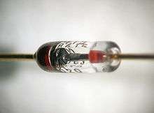
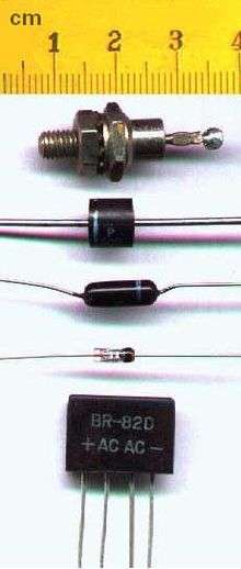
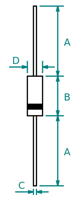
 Typical diode packages in same alignment as diode symbol. Thin bar depicts the cathode.

Point-contact diodes
A point-contact diode works the same as the junction diodes described below, but its construction is simpler. A pointed metal wire is placed in contact with an n-type semiconductor. Some metal migrates into the semiconductor to make a small p-type region around the contact. The 1N34 germanium version is still used in radio receivers as a detector and occasionally in specialized analog electronics.
Junction diodes
p–n junction diode
A p–n junction diode is made of a crystal of semiconductor, usually silicon, but germanium and gallium arsenide are also used. Impurities are added to it to create a region on one side that contains negative charge carriers (electrons), called an n-type semiconductor, and a region on the other side that contains positive charge carriers (holes), called a p-type semiconductor. When the n-type and p-type materials are attached together, a momentary flow of electrons occur from the n to the p side resulting in a third region between the two where no charge carriers are present. This region is called the depletion region because there are no charge carriers (neither electrons nor holes) in it. The diode's terminals are attached to the n-type and p-regions. The boundary between these two regions, called a p–n junction, is where the action of the diode takes place. When a sufficiently higher electrical potential is applied to the P side (the anode) than to the N side (the cathode), it allows electrons to flow through the depletion region from the N-type side to the P-type side. The junction does not allow the flow of electrons in the opposite direction when the potential is applied in reverse, creating, in a sense, an electrical check valve.
Schottky diode
Another type of junction diode, the Schottky diode, is formed from a metal–semiconductor junction rather than a p–n junction, which reduces capacitance and increases switching speed.
Current–voltage characteristic

A semiconductor diode's behavior in a circuit is given by its current–voltage characteristic, or I–V graph (see graph below). The shape of the curve is determined by the transport of charge carriers through the so-called depletion layer or depletion region that exists at the p–n junction between differing semiconductors. When a p–n junction is first created, conduction-band (mobile) electrons from the N-doped region diffuse into the P-doped region where there is a large population of holes (vacant places for electrons) with which the electrons "recombine". When a mobile electron recombines with a hole, both hole and electron vanish, leaving behind an immobile positively charged donor (dopant) on the N side and negatively charged acceptor (dopant) on the P side. The region around the p–n junction becomes depleted of charge carriers and thus behaves as an insulator.
However, the width of the depletion region (called the depletion width) cannot grow without limit. For each electron–hole pair recombination made, a positively charged dopant ion is left behind in the N-doped region, and a negatively charged dopant ion is created in the P-doped region. As recombination proceeds and more ions are created, an increasing electric field develops through the depletion zone that acts to slow and then finally stop recombination. At this point, there is a "built-in" potential across the depletion zone.
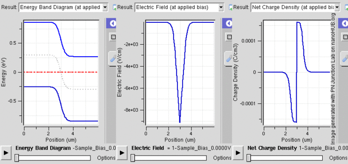
Reverse bias
If an external voltage is placed across the diode with the same polarity as the built-in potential, the depletion zone continues to act as an insulator, preventing any significant electric current flow (unless electron–hole pairs are actively being created in the junction by, for instance, light; see photodiode). This is called the reverse bias phenomenon.
Forward bias
However, if the polarity of the external voltage opposes the built-in potential, recombination can once again proceed, resulting in a substantial electric current through the p–n junction (i.e. substantial numbers of electrons and holes recombine at the junction). For silicon diodes, the built-in potential is approximately 0.7 V (0.3 V for germanium and 0.2 V for Schottky). Thus, if an external voltage greater than and opposite to the built-in voltage is applied, a current will flow and the diode is said to be "turned on" as it has been given an external forward bias. The diode is commonly said to have a forward "threshold" voltage, above which it conducts and below which conduction stops. However, this is only an approximation as the forward characteristic is according to the Shockley equation absolutely smooth (see graph below).
A diode's I–V characteristic can be approximated by four regions of operation:
- At very large reverse bias, beyond the peak inverse voltage or PIV, a process called reverse breakdown occurs that causes a large increase in current (i.e., a large number of electrons and holes are created at, and move away from the p–n junction) that usually damages the device permanently. The avalanche diode is deliberately designed for use in that manner. In the Zener diode, the concept of PIV is not applicable. A Zener diode contains a heavily doped p–n junction allowing electrons to tunnel from the valence band of the p-type material to the conduction band of the n-type material, such that the reverse voltage is "clamped" to a known value (called the Zener voltage), and avalanche does not occur. Both devices, however, do have a limit to the maximum current and power they can withstand in the clamped reverse-voltage region. Also, following the end of forward conduction in any diode, there is reverse current for a short time. The device does not attain its full blocking capability until the reverse current ceases.
- For a bias less than the PIV, the reverse current is very small. For a normal P–N rectifier diode, the reverse current through the device in the micro-ampere (µA) range is very low. However, this is temperature dependent, and at sufficiently high temperatures, a substantial amount of reverse current can be observed (mA or more).
- With a small forward bias, where only a small forward current is conducted, the current–voltage curve is exponential in accordance with the ideal diode equation. There is a definite forward voltage at which the diode starts to conduct significantly. This is called the knee voltage or cut-in voltage and is equal to the barrier potential of the p-n junction. This is a feature of the exponential curve, and appears sharper on a current scale more compressed than in the diagram shown here.
- At larger forward currents the current-voltage curve starts to be dominated by the ohmic resistance of the bulk semiconductor. The curve is no longer exponential, it is asymptotic to a straight line whose slope is the bulk resistance. This region is particularly important for power diodes. The diode can be modeled as an ideal diode in series with a fixed resistor.
In a small silicon diode operating at its rated currents, the voltage drop is about 0.6 to 0.7 volts. The value is different for other diode types—Schottky diodes can be rated as low as 0.2 V, germanium diodes 0.25 to 0.3 V, and red or blue light-emitting diodes (LEDs) can have values of 1.4 V and 4.0 V respectively.
At higher currents the forward voltage drop of the diode increases. A drop of 1 V to 1.5 V is typical at full rated current for power diodes.
Shockley diode equation
The Shockley ideal diode equation or the diode law (named after transistor co-inventor William Bradford Shockley) gives the I–V characteristic of an ideal diode in either forward or reverse bias (or no bias). The following equation is called the Shockley ideal diode equation when n, the ideality factor, is set equal to 1 :

where
- I is the diode current,
- IS is the reverse bias saturation current (or scale current),
- VD is the voltage across the diode,
- VT is the thermal voltage, and
- n is the ideality factor, also known as the quality factor or sometimes emission coefficient. The ideality factor n typically varies from 1 to 2 (though can in some cases be higher), depending on the fabrication process and semiconductor material and is set equal to 1 for the case of an "ideal" diode (thus the n is sometimes omitted). The ideality factor was added to account for imperfect junctions as observed in real transistors. The factor mainly accounts for carrier recombination as the charge carriers cross the depletion region.
The thermal voltage VT is approximately 25.85 mV at 300 K, a temperature close to "room temperature" commonly used in device simulation software. At any temperature it is a known constant defined by:

where k is the Boltzmann constant, T is the absolute temperature of the p–n junction, and q is the magnitude of charge of an electron (the elementary charge).
The reverse saturation current, IS, is not constant for a given device, but varies with temperature; usually more significantly than VT, so that VD typically decreases as T increases.
The Shockley ideal diode equation or the diode law is derived with the assumption that the only processes giving rise to the current in the diode are drift (due to electrical field), diffusion, and thermal recombination–generation (R–G) (this equation is derived by setting n = 1 above). It also assumes that the R–G current in the depletion region is insignificant. This means that the Shockley ideal diode equation doesn't account for the processes involved in reverse breakdown and photon-assisted R–G. Additionally, it doesn't describe the "leveling off" of the I–V curve at high forward bias due to internal resistance. Introducing the ideality factor, n, accounts for recombination and generation of carriers.
Under reverse bias voltages the exponential in the diode equation is negligible, and the current is a constant (negative) reverse current value of −IS. The reverse breakdown region is not modeled by the Shockley diode equation.
For even rather small forward bias voltages the exponential is very large, since the thermal voltage is very small in comparison. The subtracted '1' in the diode equation is then negligible and the forward diode current can be approximated by

The use of the diode equation in circuit problems is illustrated in the article on diode modeling.
Small-signal behavior
For circuit design, a small-signal model of the diode behavior often proves useful. A specific example of diode modeling is discussed in the article on small-signal circuits.
Reverse-recovery effect
Following the end of forward conduction in a p–n type diode, a reverse current can flow for a short time. The device does not attain its blocking capability until the mobile charge in the junction is depleted.
The effect can be significant when switching large currents very quickly.[18] A certain amount of "reverse recovery time" tr (on the order of tens of nanoseconds to a few microseconds) may be required to remove the reverse recovery charge Qr from the diode. During this recovery time, the diode can actually conduct in the reverse direction. This might give rise to a large constant current in the reverse direction for a short time while the diode is reverse biased. The magnitude of such a reverse current is determined by the operating circuit (i.e., the series resistance) and the diode is said to be in the storage-phase.[19] In certain real-world cases it is important to consider the losses that are incurred by this non-ideal diode effect.[20] However, when the slew rate of the current is not so severe (e.g. Line frequency) the effect can be safely ignored. For most applications, the effect is also negligible for Schottky diodes.
The reverse current ceases abruptly when the stored charge is depleted; this abrupt stop is exploited in step recovery diodes for generation of extremely short pulses.
Types of semiconductor diode

There are several types of p–n junction diodes, which emphasize either a different physical aspect of a diode often by geometric scaling, doping level, choosing the right electrodes, are just an application of a diode in a special circuit, or are really different devices like the Gunn and laser diode and the MOSFET:
Normal (p–n) diodes, which operate as described above, are usually made of doped silicon or, more rarely, germanium. Before the development of silicon power rectifier diodes, cuprous oxide and later selenium was used. Their low efficiency required a much higher forward voltage to be applied (typically 1.4 to 1.7 V per "cell", with multiple cells stacked so as to increase the peak inverse voltage rating for application in high voltage rectifiers), and required a large heat sink (often an extension of the diode's metal substrate), much larger than the later silicon diode of the same current ratings would require. The vast majority of all diodes are the p–n diodes found in CMOS integrated circuits, which include two diodes per pin and many other internal diodes.
- Avalanche diodes
- These are diodes that conduct in the reverse direction when the reverse bias voltage exceeds the breakdown voltage. These are electrically very similar to Zener diodes (and are often mistakenly called Zener diodes), but break down by a different mechanism: the avalanche effect. This occurs when the reverse electric field applied across the p–n junction causes a wave of ionization, reminiscent of an avalanche, leading to a large current. Avalanche diodes are designed to break down at a well-defined reverse voltage without being destroyed. The difference between the avalanche diode (which has a reverse breakdown above about 6.2 V) and the Zener is that the channel length of the former exceeds the mean free path of the electrons, resulting in many collisions between them on the way through the channel. The only practical difference between the two types is they have temperature coefficients of opposite polarities.
- Cat's whisker or crystal diodes
- These are a type of point-contact diode. The cat's whisker diode consists of a thin or sharpened metal wire pressed against a semiconducting crystal, typically galena or a piece of coal. The wire forms the anode and the crystal forms the cathode. Cat's whisker diodes were also called crystal diodes and found application in the earliest radios called crystal radio receivers. Cat's whisker diodes are generally obsolete, but may be available from a few manufacturers.
- Constant current diodes
- These are actually JFETs[21] with the gate shorted to the source, and function like a two-terminal current-limiting analog to the voltage-limiting Zener diode. They allow a current through them to rise to a certain value, and then level off at a specific value. Also called CLDs, constant-current diodes, diode-connected transistors, or current-regulating diodes.
- Esaki or tunnel diodes
- These have a region of operation showing negative resistance caused by quantum tunneling,[22] allowing amplification of signals and very simple bistable circuits. Because of the high carrier concentration, tunnel diodes are very fast, may be used at low (mK) temperatures, high magnetic fields, and in high radiation environments.[23] Because of these properties, they are often used in spacecraft.
- Gunn diodes
- These are similar to tunnel diodes in that they are made of materials such as GaAs or InP that exhibit a region of negative differential resistance. With appropriate biasing, dipole domains form and travel across the diode, allowing high frequency microwave oscillators to be built.
- Light-emitting diodes (LEDs)
- In a diode formed from a direct band-gap semiconductor, such as gallium arsenide, charge carriers that cross the junction emit photons when they recombine with the majority carrier on the other side. Depending on the material, wavelengths (or colors)[24] from the infrared to the near ultraviolet may be produced.[25] The forward potential of these diodes depends on the wavelength of the emitted photons: 2.1 V corresponds to red, 4.0 V to violet. The first LEDs were red and yellow, and higher-frequency diodes have been developed over time. All LEDs produce incoherent, narrow-spectrum light; "white" LEDs are actually combinations of three LEDs of a different color, or a blue LED with a yellow scintillator coating. LEDs can also be used as low-efficiency photodiodes in signal applications. An LED may be paired with a photodiode or phototransistor in the same package, to form an opto-isolator.
- Laser diodes
- When an LED-like structure is contained in a resonant cavity formed by polishing the parallel end faces, a laser can be formed. Laser diodes are commonly used in optical storage devices and for high speed optical communication.
- Thermal diodes
- This term is used both for conventional p–n diodes used to monitor temperature because of their varying forward voltage with temperature, and for Peltier heat pumps for thermoelectric heating and cooling. Peltier heat pumps may be made from semiconductor, though they do not have any rectifying junctions, they use the differing behaviour of charge carriers in N and P type semiconductor to move heat.
- Perun's diodes
- This is a special type of voltage-surge protection diode. It is characterized by the symmetrical voltage-current characteristic, similar to DIAC. It has much faster response time however, that's why it is used in demanding applications.
- Photodiodes
- All semiconductors are subject to optical charge carrier generation. This is typically an undesired effect, so most semiconductors are packaged in light blocking material. Photodiodes are intended to sense light(photodetector), so they are packaged in materials that allow light to pass, and are usually PIN (the kind of diode most sensitive to light).[26] A photodiode can be used in solar cells, in photometry, or in optical communications. Multiple photodiodes may be packaged in a single device, either as a linear array or as a two-dimensional array. These arrays should not be confused with charge-coupled devices.
- PIN diodes
- A PIN diode has a central un-doped, or intrinsic, layer, forming a p-type/intrinsic/n-type structure.[27] They are used as radio frequency switches and attenuators. They are also used as large-volume, ionizing-radiation detectors and as photodetectors. PIN diodes are also used in power electronics, as their central layer can withstand high voltages. Furthermore, the PIN structure can be found in many power semiconductor devices, such as IGBTs, power MOSFETs, and thyristors.
- Schottky diodes
- Schottky diodes are constructed from a metal to semiconductor contact. They have a lower forward voltage drop than p–n junction diodes. Their forward voltage drop at forward currents of about 1 mA is in the range 0.15 V to 0.45 V, which makes them useful in voltage clamping applications and prevention of transistor saturation. They can also be used as low loss rectifiers, although their reverse leakage current is in general higher than that of other diodes. Schottky diodes are majority carrier devices and so do not suffer from minority carrier storage problems that slow down many other diodes—so they have a faster reverse recovery than p–n junction diodes. They also tend to have much lower junction capacitance than p–n diodes, which provides for high switching speeds and their use in high-speed circuitry and RF devices such as switched-mode power supply, mixers, and detectors.
- Super barrier diodes
- Super barrier diodes are rectifier diodes that incorporate the low forward voltage drop of the Schottky diode with the surge-handling capability and low reverse leakage current of a normal p–n junction diode.
- Gold-doped diodes
- As a dopant, gold (or platinum) acts as recombination centers, which helps a fast recombination of minority carriers. This allows the diode to operate at signal frequencies, at the expense of a higher forward voltage drop. Gold-doped diodes are faster than other p–n diodes (but not as fast as Schottky diodes). They also have less reverse-current leakage than Schottky diodes (but not as good as other p–n diodes).[28][29] A typical example is the 1N914.
- Snap-off or Step recovery diodes
- The term step recovery relates to the form of the reverse recovery characteristic of these devices. After a forward current has been passing in an SRD and the current is interrupted or reversed, the reverse conduction will cease very abruptly (as in a step waveform). SRDs can, therefore, provide very fast voltage transitions by the very sudden disappearance of the charge carriers.
- Stabistors or Forward Reference Diodes
- The term stabistor refers to a special type of diodes featuring extremely stable forward voltage characteristics. These devices are specially designed for low-voltage stabilization applications requiring a guaranteed voltage over a wide current range and highly stable over temperature.
- Transient voltage suppression diode (TVS)
- These are avalanche diodes designed specifically to protect other semiconductor devices from high-voltage transients.[30] Their p–n junctions have a much larger cross-sectional area than those of a normal diode, allowing them to conduct large currents to ground without sustaining damage.
- Varicap or varactor diodes
- These are used as voltage-controlled capacitors. These are important in PLL (phase-locked loop) and FLL (frequency-locked loop) circuits, allowing tuning circuits, such as those in television receivers, to lock quickly on to the frequency. They also enabled tunable oscillators in early discrete tuning of radios, where a cheap and stable, but fixed-frequency, crystal oscillator provided the reference frequency for a voltage-controlled oscillator.
- Zener diodes
- These can be made to conduct in reverse bias (backward), and are correctly termed reverse breakdown diodes. This effect, called Zener breakdown, occurs at a precisely defined voltage, allowing the diode to be used as a precision voltage reference. The term Zener diode is colloquially applied to several types of breakdown diodes, but strictly speaking Zener diodes have a breakdown voltage of below 5 volts, whilst avalanche diodes are used for breakdown voltages above that value. In practical voltage reference circuits, Zener and switching diodes are connected in series and opposite directions to balance the temperature coefficient response of the diodes to near-zero. Some devices labeled as high-voltage Zener diodes are actually avalanche diodes (see above). Two (equivalent) Zeners in series and in reverse order, in the same package, constitute a transient absorber (or Transorb, a registered trademark).
Other uses for semiconductor diodes include the sensing of temperature, and computing analog logarithms (see Operational amplifier applications#Logarithmic output).
Numbering and coding schemes
There are a number of common, standard and manufacturer-driven numbering and coding schemes for diodes; the two most common being the EIA/JEDEC standard and the European Pro Electron standard:
EIA/JEDEC
The standardized 1N-series numbering EIA370 system was introduced in the US by EIA/JEDEC (Joint Electron Device Engineering Council) about 1960. Most diodes have a 1-prefix designation (e.g., 1N4003). Among the most popular in this series were: 1N34A/1N270 (germanium signal), 1N914/1N4148 (silicon signal), 1N400x (silicon 1A power rectifier), and 1N580x (silicon 3A power rectifier).[31][32][33]
JIS
The JIS semiconductor designation system has all semiconductor diode designations starting with "1S".
Pro Electron
The European Pro Electron coding system for active components was introduced in 1966 and comprises two letters followed by the part code. The first letter represents the semiconductor material used for the component (A = germanium and B = silicon) and the second letter represents the general function of the part (for diodes, A = low-power/signal, B = variable capacitance, X = multiplier, Y = rectifier and Z = voltage reference); for example:
- AA-series germanium low-power/signal diodes (e.g., AA119)
- BA-series silicon low-power/signal diodes (e.g., BAT18 silicon RF switching diode)
- BY-series silicon rectifier diodes (e.g., BY127 1250V, 1A rectifier diode)
- BZ-series silicon Zener diodes (e.g., BZY88C4V7 4.7V Zener diode)
Other common numbering / coding systems (generally manufacturer-driven) include:
- GD-series germanium diodes (e.g., GD9) – this is a very old coding system
- OA-series germanium diodes (e.g., OA47) – a coding sequence developed by Mullard, a UK company
As well as these common codes, many manufacturers or organisations have their own systems too – for example:
- HP diode 1901-0044 = JEDEC 1N4148
- UK military diode CV448 = Mullard type OA81 = GEC type GEX23
Related devices
In optics, an equivalent device for the diode but with laser light would be the Optical isolator, also known as an Optical Diode, that allows light to only pass in one direction. It uses a Faraday rotator as the main component.
Applications
Radio demodulation
The first use for the diode was the demodulation of amplitude modulated (AM) radio broadcasts. The history of this discovery is treated in depth in the radio article. In summary, an AM signal consists of alternating positive and negative peaks of a radio carrier wave, whose amplitude or envelope is proportional to the original audio signal. The diode (originally a crystal diode) rectifies the AM radio frequency signal, leaving only the positive peaks of the carrier wave. The audio is then extracted from the rectified carrier wave using a simple filter and fed into an audio amplifier or transducer, which generates sound waves.
Power conversion

Rectifiers are constructed from diodes, where they are used to convert alternating current (AC) electricity into direct current (DC). Automotive alternators are a common example, where the diode, which rectifies the AC into DC, provides better performance than the commutator or earlier, dynamo. Similarly, diodes are also used in Cockcroft–Walton voltage multipliers to convert AC into higher DC voltages.
Over-voltage protection
Diodes are frequently used to conduct damaging high voltages away from sensitive electronic devices. They are usually reverse-biased (non-conducting) under normal circumstances. When the voltage rises above the normal range, the diodes become forward-biased (conducting). For example, diodes are used in (stepper motor and H-bridge) motor controller and relay circuits to de-energize coils rapidly without the damaging voltage spikes that would otherwise occur. (A diode used in such an application is called a flyback diode). Many integrated circuits also incorporate diodes on the connection pins to prevent external voltages from damaging their sensitive transistors. Specialized diodes are used to protect from over-voltages at higher power (see Diode types above).
Logic gates
Diodes can be combined with other components to construct AND and OR logic gates. This is referred to as diode logic.
Ionizing radiation detectors
In addition to light, mentioned above, semiconductor diodes are sensitive to more energetic radiation. In electronics, cosmic rays and other sources of ionizing radiation cause noise pulses and single and multiple bit errors. This effect is sometimes exploited by particle detectors to detect radiation. A single particle of radiation, with thousands or millions of electron volts of energy, generates many charge carrier pairs, as its energy is deposited in the semiconductor material. If the depletion layer is large enough to catch the whole shower or to stop a heavy particle, a fairly accurate measurement of the particle's energy can be made, simply by measuring the charge conducted and without the complexity of a magnetic spectrometer, etc. These semiconductor radiation detectors need efficient and uniform charge collection and low leakage current. They are often cooled by liquid nitrogen. For longer-range (about a centimetre) particles, they need a very large depletion depth and large area. For short-range particles, they need any contact or un-depleted semiconductor on at least one surface to be very thin. The back-bias voltages are near breakdown (around a thousand volts per centimetre). Germanium and silicon are common materials. Some of these detectors sense position as well as energy. They have a finite life, especially when detecting heavy particles, because of radiation damage. Silicon and germanium are quite different in their ability to convert gamma rays to electron showers.
Semiconductor detectors for high-energy particles are used in large numbers. Because of energy loss fluctuations, accurate measurement of the energy deposited is of less use.
Temperature measurements
A diode can be used as a temperature measuring device, since the forward voltage drop across the diode depends on temperature, as in a silicon bandgap temperature sensor. From the Shockley ideal diode equation given above, it might appear that the voltage has a positive temperature coefficient (at a constant current), but usually the variation of the reverse saturation current term is more significant than the variation in the thermal voltage term. Most diodes therefore have a negative temperature coefficient, typically −2 mV/˚C for silicon diodes. The temperature coefficient is approximately constant for temperatures above about 20 kelvins. Some graphs are given for 1N400x series,[34] and CY7 cryogenic temperature sensor.[35]
Current steering
Diodes will prevent currents in unintended directions. To supply power to an electrical circuit during a power failure, the circuit can draw current from a battery. An uninterruptible power supply may use diodes in this way to ensure that current is only drawn from the battery when necessary. Likewise, small boats typically have two circuits each with their own battery/batteries: one used for engine starting; one used for domestics. Normally, both are charged from a single alternator, and a heavy-duty split-charge diode is used to prevent the higher-charge battery (typically the engine battery) from discharging through the lower-charge battery when the alternator is not running.
Diodes are also used in electronic musical keyboards. To reduce the amount of wiring needed in electronic musical keyboards, these instruments often use keyboard matrix circuits. The keyboard controller scans the rows and columns to determine which note the player has pressed. The problem with matrix circuits is that, when several notes are pressed at once, the current can flow backwards through the circuit and trigger "phantom keys" that cause "ghost" notes to play. To avoid triggering unwanted notes, most keyboard matrix circuits have diodes soldered with the switch under each key of the musical keyboard. The same principle is also used for the switch matrix in solid-state pinball machines.
Waveform Clipper
Diodes can be used to limit the positive or negative excursion of a signal to a prescribed voltage.
Clamper
A diode clamp circuit can take a periodic alternating current signal that oscillates between positive and negative values, and vertically displace it such that either the positive, or the negative peaks occur at a prescribed level. The clamper does not restrict the peak-to-peak excursion of the signal, it moves the whole signal up or down so as to place the peaks at the reference level.
Abbreviations
Diodes are usually referred to as D for diode on PCBs. Sometimes the abbreviation CR for crystal rectifier is used.[36]
See also
References
- ↑ Tooley, Mike (2012). Electronic Circuits: Fundamentals and Applications, 3rd Ed. Routlege. p. 81. ISBN 1-136-40731-6.
- ↑ Lowe, Doug (2013). "Electronics Components: Diodes". Electronics All-In-One Desk Reference For Dummies. John Wiley & Sons. Retrieved January 4, 2013.
- ↑ Crecraft, David; Stephen Gergely (2002). Analog Electronics: Circuits, Systems and Signal Processing. Butterworth-Heinemann. p. 110. ISBN 0-7506-5095-8.
- ↑ Horowitz, Paul; Winfield Hill (1989). The Art of Electronics, 2nd Ed. London: Cambridge University Press. p. 44. ISBN 0-521-37095-7.
- ↑ "Physical Explanation – General Semiconductors". 2010-05-25. Retrieved 2010-08-06.
- ↑ "The Constituents of Semiconductor Components". 2010-05-25. Retrieved 2010-08-06.
- ↑ Guthrie, Frederick (October 1873) "On a relation between heat and static electricity," The London, Edinburgh and Dublin Philosophical Magazine and Journal of Science, 4th series, 46 : 257–266.
- ↑ 1928 Nobel Lecture: Owen W. Richardson, "Thermionic phenomena and the laws which govern them", December 12, 1929
- ↑ Edison, Thomas A. "Electrical Meter" U.S. Patent 307,030 Issue date: Oct 21, 1884
- ↑ "Road to the Transistor". Jmargolin.com. Retrieved 2008-09-22.
- ↑ Braun, Ferdinand (1874) "Ueber die Stromleitung durch Schwefelmetalle" (On current conduction in metal sulphides), Annalen der Physik und Chemie, 153 : 556–563.
- ↑ Karl Ferdinand Braun. chem.ch.huji.ac.il
- ↑ "Diode". Encyclobeamia.solarbotics.net.
- ↑ Sarkar, Tapan K. (2006). History of wireless. USA: John Wiley and Sons. pp. 94, 291–308. ISBN 0-471-71814-9.
- ↑ Pickard, Greenleaf Whittier "Means for receiving intelligence communicated by electric waves" U.S. Patent 836,531 Issued: August 30, 1906
- ↑ Choi, Charles Q. (4 April 2016) World's Smallest Diode Is Made of DNA. IEEE Spectrum
- ↑ Emmino, Nicolette (5 April 2016) The World’s Smallest Diode Has Been Developed. IHS Electronics360
- ↑ Diode reverse recovery in a boost converter. ECEN5817. ecee.colorado.edu
- ↑ Elhami Khorasani, A.; Griswold, M.; Alford, T. L. (2014). "Gate-Controlled Reverse Recovery for Characterization of LDMOS Body Diode". IEEE Electron Device Letters. 35 (11): 1079. Bibcode:2014IEDL...35.1079E. doi:10.1109/LED.2014.2353301.
- ↑ Inclusion of Switching Loss in the Averaged Equivalent Circuit Model. ECEN5797. ecee.colorado.edu
- ↑ Current regulator diodes. Digikey.com (2009-05-27). Retrieved 2013-12-19.
- ↑ Jonscher, A. K. (1961). "The physics of the tunnel diode". British Journal of Applied Physics. 12 (12): 654. Bibcode:1961BJAP...12..654J. doi:10.1088/0508-3443/12/12/304.
- ↑ Dowdey, J. E.; Travis, C. M. (1964). "An Analysis of Steady-State Nuclear Radiation Damage of Tunnel Diodes". IEEE Transactions on Nuclear Science. 11 (5): 55. Bibcode:1964ITNS...11...55D. doi:10.1109/TNS2.1964.4315475.
- ↑ Classification of components. Digikey.com (2009-05-27). Retrieved 2013-12-19.
- ↑ "Component Construction". 2010-05-25. Retrieved 2010-08-06.
- ↑ Component Construction. Digikey.com (2009-05-27). Retrieved 2013-12-19.
- ↑ "Physics and Technology". 2010-05-25. Retrieved 2010-08-06.
- ↑ Fast Recovery Epitaxial Diodes (FRED) Characteristics – Applications – Examples. (PDF). Retrieved 2013-12-19.
- ↑ Sze, S. M. (1998) Modern Semiconductor Device Physics, Wiley Interscience, ISBN 0-471-15237-4
- ↑ Protecting Low Current Loads in Harsh Electrical Environments. Digikey.com (2009-05-27). Retrieved 2013-12-19.
- ↑ "About JEDEC". Jedec.org. Retrieved 2008-09-22.
- ↑ "Introduction dates of common transistors and diodes?". EDAboard.com. 2010-06-10. Archived from the original on October 11, 2007. Retrieved 2010-08-06.
- ↑ I.D.E.A. "Transistor Museum Construction Projects Point Contact Germanium Western Electric Vintage Historic Semiconductors Photos Alloy Junction Oral History". Semiconductormuseum.com. Retrieved 2008-09-22.
- ↑ 1N400x Diode Family Forward Voltage. Cliftonlaboratories.com. Retrieved 2013-12-19.
- ↑ Cryogenic Temperature Sensors. omega.com
- ↑ John Ambrose Fleming (1919). The Principles of Electric Wave Telegraphy and Telephony. London: Longmans, Green. p. 550.
External links
| Wikimedia Commons has media related to Diodes. |
- Diodes and Rectifiers – Chapter on All About Circuits
- Structure and Functional Behavior of PIN Diodes – PowerGuru
- Interactive and animations
- Interactive Explanation of Semiconductor Diode, University of Cambridge
- Schottky Diode Flash Tutorial Animation
- Datasheets
- Discrete Databook (Historical 1978), National Semiconductor (now Texas Instruments)
- Discrete Databook (Historical 1982), SGS (now STMicroelectronics)
- Discrete Databook (Historical 1985), Fairchild