Bipolar transistor biasing
Bipolar transistor amplifiers must be properly biased to operate correctly. In circuits made with individual devices (discrete circuits), biasing networks consisting of resistors are commonly employed. Much more elaborate biasing arrangements are used in integrated circuits, for example, bandgap voltage references and current mirrors.
The operating point of a device, also known as bias point, quiescent point, or Q-point, is the point on the output characteristics that shows the DC collector–emitter voltage (Vce) and the collector current (Ic) with no input signal applied. The term is normally used in connection with devices such as transistors.
Bias circuit requirements
Signal requirements for class-A amplifiers
For analog operation of a class-A amplifier, the Q-point is placed so the transistor stays in active mode (does not shift to operation in the saturation region or cut-off region) when input is applied. For digital operation, the Q-point is placed so the transistor does the contrary – switches from the "on" (saturation) to the "off" (cutoff) state. Often, the Q-point is established near the center of the active region of a transistor characteristic to allow similar signal swings in positive and negative directions. The Q-point should be stable; in particular, it should be insensitive to variations in transistor parameters (for example, should not shift if transistor is replaced by another of the same type), variations in temperature, variations in power supply voltage and so forth. The circuit must also be practical; both easily implemented and cost-effective.
Thermal considerations
At constant current, the voltage across the emitter–base junction VBE of a bipolar transistor decreases 2 mV (silicon) and 1.8mV (germanium) for each 1 °C rise in temperature (reference being 25 °C). By the Ebers–Moll model, if the base–emitter voltage VBE is held constant and the temperature rises, the current through the base–emitter diode IB will increase, and thus the collector current IC will also increase. Depending on the bias point, the power dissipated in the transistor may also increase, which will further increase its temperature and exacerbate the problem. This deleterious positive feedback results in thermal runaway.[1] There are several approaches to mitigate bipolar transistor thermal runaway. For example,
- Negative feedback can be built into the biasing circuit so that increased collector current leads to decreased base current. Hence, the increasing collector current throttles its source.
- Heat sinks can be used that carry away extra heat and prevent the base–emitter temperature from rising.
- The transistor can be biased so that its collector is normally less than half of the power supply voltage, which implies that collector–emitter power dissipation is at its maximum value. Runaway is then impossible because increasing collector current leads to a decrease in dissipated power; this notion is known as the half-voltage principle.
The circuits below primarily demonstrate the use of negative feedback to prevent thermal runaway.
Types of bias circuit for class-A amplifiers
The following discussion treats five common biasing circuits used with class-A bipolar transistor amplifiers:
- Fixed bias
- Collector-to-base bias
- Fixed bias with emitter resistor
- Voltage divider bias or potential divider
- Emitter bias
Fixed bias (base bias)

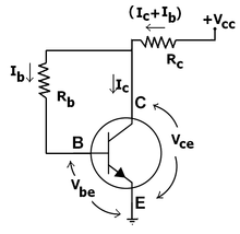
This form of biasing is also called base bias or fixed resistance baising. In the example image on the right, the single power source (for example, a battery) is used for both collector and base of a transistor, although separate batteries can also be used.
In the given circuit,
- Vcc = IBRB + Vbe
Therefore,
- IB = (Vcc − Vbe)/RB
For a given transistor, Vbe does not vary significantly during use. As Vcc is of fixed value, on selection of RB, the base current IB is fixed. Therefore, this type is called fixed bias type of circuit.
Also for given circuit,
- Vcc = ICRC + Vce
Therefore,
- Vce = Vcc − ICRC
The common-emitter current gain of a transistor is an important parameter in circuit design, and is specified on the data sheet for a particular transistor. It is denoted as β on this page.
Because
- IC = βIB
we can obtain IC as well. In this manner, operating point given as (Vce,IC) can be set for given transistor.
Merits:
- It is simple to shift the operating point anywhere in the active region by merely changing the base resistor (RB).
- A very small number of components are required.
Demerits:
- The collector current does not remain constant with variation in temperature or power supply voltage. Therefore, the operating point is unstable.
- Changes in Vbe will change IB and thus cause IE to change. This in turn will alter the gain of the stage.
- When the transistor is replaced with another one, considerable change in the value of β can be expected. Due to this change the operating point will shift.
- For small-signal transistors (e.g., not power transistors) with relatively high values of β (i.e., between 100 and 200), this configuration will be prone to thermal runaway. In particular, the stability factor, which is a measure of the change in collector current with changes in reverse saturation current, is approximately β+1. To ensure absolute stability of the amplifier, a stability factor of less than 25 is preferred, and so small-signal transistors have large stability factors.
Usage:
Due to the above inherent drawbacks, fixed bias is rarely used in linear circuits (i.e., those circuits which use the transistor as a current source). Instead, it is often used in circuits where transistor is used as a switch. However, one application of fixed bias is to achieve crude automatic gain control in the transistor by feeding the base resistor from a DC signal derived from the AC output of a later stage.
Collector feedback bias
This configuration employs negative feedback to prevent thermal runaway and stabilize the operating point. In this form of biasing, the base resistor is connected to the collector instead of connecting it to the DC source . So any thermal runaway will induce a voltage drop across the resistor that will throttle the transistor's base current.


From Kirchhoff's voltage law, the voltage across the base resistor is


By the Ebers–Moll model, , and so


From Ohm's law, the base current , and so


Hence, the base current is


If is held constant and temperature increases, then the collector current increases. However, a larger causes the voltage drop across resistor to increase, which in turn reduces the voltage across the base resistor . A lower base-resistor voltage drop reduces the base current , which results in less collector current . Because an increase in collector current with temperature is opposed, the operating point is kept stable.


Merits:
- Circuit stabilizes the operating point against variations in temperature and β (i.e. replacement of transistor).
- Circuit stabilizes the operating point (as a fraction of ) against variations in .
Demerits:
- Although small changes in β are OK, large changes in β will greatly change the operating point. must be chosen once β is known fairly accurately (perhaps within ~ 25%), yet the variability of β between "identical" parts is often larger than this.
- In this circuit, to keep independent of , the following condition must be met:


which is the case when

- As -value is fixed (and generally unknown) for a given transistor, this relation can be satisfied either by keeping fairly large or making very low.
- If is large, a high is necessary, which increases cost as well as precautions necessary while handling.
- If is low, the reverse bias of the collector–base region is small, which limits the range of collector voltage swing that leaves the transistor in active mode.
- The resistor causes an AC feedback, reducing the voltage gain of the amplifier. This undesirable effect is a trade-off for greater Q-point stability. However, a T (R-C-R) network can be used to reduce the AC feedback, which however poses a heavier load on the collector than the simple feedback resistor. At higher frequencies a R-L feedback network can be used, however, it will introduce peaking into the frequency response at various points.
Usage: The negative feedback also increases the input impedance of the amplifier as seen from the base, which can be advantageous. Due to the gain reduction from feedback, this biasing form is used only when the trade-off for stability is warranted.
Fixed bias with emitter resistor

The fixed bias circuit is modified by attaching an external resistor to the emitter. This resistor introduces negative feedback that stabilizes the Q-point. From Kirchhoff's voltage law, the voltage across the base resistor is

From Ohm's law, the base current is

The way feedback controls the bias point is as follows. If Vbe is held constant and temperature increases, emitter current increases. However, a larger Ie increases the emitter voltage Ve = IeRe, which in turn reduces the voltage VRb across the base resistor. A lower base-resistor voltage drop reduces the base current, which results in less collector current because Ic = β IB. Collector current and emitter current are related by Ic = α Ie with α ≈ 1, so the increase in emitter current with temperature is opposed, and the operating point is kept stable.
Similarly, if the transistor is replaced by another, there may be a change in IC (corresponding to change in β-value, for example). By similar process as above, the change is negated and operating point kept stable.
For the given circuit,

Merits:
The circuit has the tendency to stabilize operating point against changes in temperature and β-value.
Demerits:
- In this circuit, to keep IC independent of β the following condition must be met:

which is approximately the case if

- As β-value is fixed for a given transistor, this relation can be satisfied either by keeping RE very large, or making RB very low.
- If RE is of large value, high VCC is necessary. This increases cost as well as precautions necessary while handling.
- If RB is low, a separate low voltage supply should be used in the base circuit. Using two supplies of different voltages is impractical.
- In addition to the above, RE causes AC feedback which reduces the voltage gain of the amplifier.
Usage:
The feedback also increases the input impedance of the amplifier when seen from the base, which can be advantageous. Due to the above disadvantages, this type of biasing circuit is used only with careful consideration of the trade-offs involved.
Collector-Stabilized Biasing
Voltage divider biasing or emitter bias

The voltage divider is formed using external resistors R1 and R2. The voltage across R2 forward biases the emitter junction. By proper selection of resistors R1 and R2, the operating point of the transistor can be made independent of β. In this circuit, the voltage divider holds the base voltage fixed independent of base current provided the divider current is large compared to the base current. However, even with a fixed base voltage, collector current varies with temperature (for example) so an emitter resistor is added to stabilize the Q-point, similar to the above circuits with emitter resistor.
In this circuit the base voltage is given by:
voltage across


- provided .


Also

For the given circuit,

Merits:
- Unlike above circuits, only one dc supply is necessary.
- Operating point is almost independent of β variation.
- Operating point stabilized against shift in temperature.
Demerits:
- In this circuit, to keep IC independent of β the following condition must be met:

which is approximately the case if

where R1 || R2 denotes the equivalent resistance of R1 and R2 connected in parallel.
- As β-value is fixed for a given transistor, this relation can be satisfied either by keeping RE fairly large, or making R1||R2 very low.
- If RE is of large value, high VCC is necessary. This increases cost as well as precautions necessary while handling.
- If R1 || R2 is low, either R1 is low, or R2 is low, or both are low. A low R1 raises VB closer to VC, reducing the available swing in collector voltage, and limiting how large RC can be made without driving the transistor out of active mode. A low R2 lowers Vbe, reducing the allowed collector current. Lowering both resistor values draws more current from the power supply and lowers the input resistance of the amplifier as seen from the base.
- AC as well as DC feedback is caused by RE, which reduces the AC voltage gain of the amplifier. A method to avoid AC feedback while retaining DC feedback is discussed below.
Usage:
The circuit's stability and merits as above make it widely used for linear circuits.
Voltage divider with AC bypass capacitor

The standard voltage divider circuit discussed above faces a drawback – AC feedback caused by resistor RE reduces the gain. This can be avoided by placing a capacitor (CE) in parallel with RE, as shown in circuit diagram. The result is that the DC operating point is well controlled, while the AC-gain is much higher (approaching β), rather than the much lower (but predictable) value of without the capacitor.


When a split supply (dual power supply) is available, this biasing circuit is the most effective, and provides zero bias voltage at the emitter or collector for load. The negative supply VEE is used to forward-bias the emitter junction through RE. The positive supply VCC is used to reverse-bias the collector junction. Only two resistors are necessary for the common collector stage and four resistors for the common emitter or common base stage.
We know that,
VB − VE = Vbe
If RB is small enough, base voltage will be approximately zero. Therefore, emitter current is,
IE = (VEE − Vbe)/RE
The operating point is independent of β if RE >> RB/β
Merit:
Demerit:
This type can only be used when a split (dual) power supply is available.
Class-B and AB amplifiers
Signal requirements
Class B and AB amplifiers employ 2 active devices to cover the complete 360 deg of input signal flow. Each transistor is therefore biased to perform over approximately 180 deg of the input signal. Class B bias is when the collector current Ic with no signal is just conducting (about 1% of maximum possible value). Class-AB bias is when the collector current Ic is about 1/4 of maximum possible value. The class-AB push–pull output amplifier circuit below could be the basis for a moderate-power audio amplifier.

Q3 is a common emitter stage that provides amplification of the signal and the DC bias current through D1 and D2 to generate a bias voltage for the output devices. The output pair are arranged in class-AB push–pull, also called a complementary pair. The diodes D1 and D2 provide a small amount of constant voltage bias for the output pair, just biasing them into the conducting state so that crossover distortion is minimized. That is, the diodes push the output stage into class-AB mode (assuming that the base-emitter drop of the output transistors is reduced by heat dissipation).
This design automatically stabilizes its operating point, since overall feedback internally operates from DC up through the audio range and beyond. The use of fixed diode bias requires the diodes to be both electrically and thermally matched to the output transistors. If the output transistors conduct too much, they can easily overheat and destroy themselves, as the full current from the power supply is not limited at this stage.
A common solution to help stabilize the output device operating point is to include some emitter resistors, typically an ohm or so. Calculating the values of the circuit's resistors and capacitors is done based on the components employed and the intended use of the amplifier.
See also
References
Further reading
- Patil, P.K.; Chitnis, M.M. (2005). Basic Electricity and Semiconductor Devices. Phadke Prakashan.
External links
- Bias – from Sci-Tech Encyclopedia
- Electrical Engineering Training Series: Types of bias