Via (electronics)
A via or VIA (Latin for path or way, also known as vertical interconnect access) is an electrical connection between layers in a physical electronic circuit that goes through the plane of one or more adjacent layers.
In IC
In integrated circuit design, a via is a small opening in an insulating oxide layer that allows a conductive connection between different layers. A via on an integrated circuit is often called a through-chip via. A via connecting the lowest layer of metal to diffusion or poly is typically called a "contact".
In PCB

(1) Through hole.
(2) Blind via.
(3) Buried via.
The grey and green layers are non-conducting, while the thin orange layers and vias are conductive.

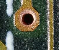
In printed circuit board design, a via consists of two pads in corresponding positions on different layers of the board, that are electrically connected by a hole through the board. The hole is made conductive by electroplating, or is lined with a tube or a rivet. High-density multi-layer PCBs may have microvias: blind vias are exposed only on one side of the board, while buried vias connect internal layers without being exposed on either surface. Thermal vias carry heat away from power devices and are typically used in arrays of about a dozen.
A via consists of:
- Barrel — conductive tube filling the drilled hole
- Pad — connects each end of the barrel to the component, plane or trace
- Antipad — clearance hole between barrel and metal layer to which it is not connected
A via may be at the edge of the board so that it is cut in half when the board is separated; this is known as a castellated hole and is used for a variety of reasons, including allowing one PCB to be soldered to another in a stack.[1]
Three major kinds of vias are shown in right figure. Basic steps of making PCB is repetition of layer stacking - through drilling of stacked one and plating - copper trace patterning using photolithography and etching. It means without depth-controlled drilling technique such as using laser, possible vias are limited depending on a way of layer stacking. PCB manufacturing typically starts with so called core, basic double-sided PCB. More than two layers are stacked from this basic building block. If two more layers are consecutively stacked from bottom of core, you can have 1-2 via, 1-3 via and through hole. Each type of via is made by drilling at each stacking stage. If one layer is firstly stacked on top of the core and other is stacked from bottom, possible vias are 1-3, 2-3 and through hole. So user must gather information of allowed way of PCB stacking or possible vias from PCB manufacturer. For cheap price, only through holes are made and antipad (or called clearance) are placed on layers which are supposed not to be contacted to vias.
Gallery
|


|
See also
| The Wikibook Practical Electronics has a page on the topic of: PCB Layout#Holes |
- Printed circuit board (PCB)
- Through-hole technology (THT)
- Surface-mount technology (SMT)
- Through-silicon via (TSV)
- Via fence
References
External links
PCB vias design guidelines
- Tips for PCB vias design – Tips for PCB vias design (Quick-teck PCBs technical note)