Scanning SQUID microscope
A Scanning SQUID Microscope is a sensitive near-field imaging system for the measurement of weak magnetic fields by moving a Superconducting Quantum Interference Device (SQUID) across an area. The microscope can map out buried current-carrying wires by measuring the magnetic fields produced by the currents, or can be used to image fields produced by magnetic materials. By mapping out the current in an integrated circuit or a package, short circuits can be localized and chip designs can be verified to see that current is flowing where expected.
High temperature scanning SQUID microscope

A high temperature Scanning SQUID Microscope using a YBCO SQUID is capable of measuring magnetic fields as small as 20 pT (about 2 million times weaker than the earth’s magnetic field). The SQUID sensor is sensitive enough that it can detect a wire even if it is carrying only 10 nA of current at a distance of 100 µm from the SQUID sensor with 1 second averaging. The microscope uses a patented design to allow the sample under investigation to be at room temperature and in air while the SQUID sensor is under vacuum and cooled to less than 80 K using a cryo cooler. No Liquid Nitrogen is used. During non-contact, non-destructive imaging of room temperature samples in air, the system achieves a raw, unprocessed spatial resolution equal to the distance separating the sensor from the current or the effective size of the sensor, whichever is larger. To best locate a wire short in a buried layer, however, a Fast Fourier Transform (FFT) back-evolution technique can be used to transform the magnetic field image into an equivalent map of the current in an integrated circuit or printed wiring board.[1][2] The resulting current map can then be compared to a circuit diagram to determine the fault location. With this post-processing of a magnetic image and the low noise present in SQUID images, it is possible to enhance the spatial resolution by factors of 5 or more over the near-field limited magnetic image. The system’s output is displayed as a false-color image of magnetic field strength or current magnitude (after processing) versus position on the sample. After processing to obtain current magnitude, this microscope has been successful at locating shorts in conductors to within ±16 µm at a sensor-current distance of 150 µm.[3]
SQUID operation
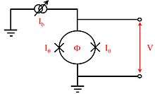

As the name implies, SQUIDs are made from superconducting material. As a result, they need to be cooled to cryogenic temperatures of less than 90 K (liquid nitrogen temperatures) for high temperature SQUIDs and less than 9 K (liquid helium temperatures) for low temperature SQUIDs. For magnetic current imaging systems, a small (about 30 µm wide) high temperature SQUID is used. This system has been designed to keep a high temperature SQUID, made from YBa2Cu3O7, cooled below 80K and in vacuum while the device under test is at room temperature and in air. A SQUID consists of two Josephson tunnel junctions that are connected together in a superconducting loop (see Figure 1). A Josephson junction is formed by two superconducting regions that are separated by a thin insulating barrier. Current exists in the junction without any voltage drop, up to a maximum value, called the critical current, Io. When the SQUID is biased with a constant current that exceeds the critical current of the junction, then changes in the magnetic flux, Φ, threading the SQUID loop produce changes in the voltage drop across the SQUID (see Figure 1). Figure 2(a) shows the I-V characteristic of a SQUID where ∆V is the modulation depth of the SQUID due to external magnetic fields. The voltage across a SQUID is a nonlinear periodic function of the applied magnetic field, with a periodicity of one flux quantum, Φ0=2.07×10⁻¹⁵ Tm2 (see Figure 2(b)). In order to convert this nonlinear response to a linear response, a negative feedback circuit is used to apply a feedback flux to the SQUID so as to keep the total flux through the SQUID constant. In such a flux locked loop, the magnitude of this feedback flux is proportional to the external magnetic field applied to the SQUID. Further description of the physics of SQUIDs and SQUID microscopy can be found elsewhere.[4][5][6][7]
Magnetic field detection using SQUID
Magnetic current imaging uses the magnetic fields produced by currents in electronic devices to obtain images of those currents. This is accomplished though the fundamental physics relationship between magnetic fields and current, the Biot-Savart Law:
- B is the magnetic induction, Idℓ is an element of the current, the constant µ0 is the permeability of free space, and r is the distance between the current and the sensor.

As a result, the current can be directly calculated from the magnetic field knowing only the separation between the current and the magnetic field sensor. The details of this mathematical calculation can be found elsewhere,[8] but what is important to know here is that this is a direct calculation that is not influenced by other materials or effects, and that through the use of Fast Fourier Transforms these calculations can be performed very quickly. A magnetic field image can be converted to a current density image in about 1 or 2 seconds.
Applications using a Scanning SQUID Microscope
Scanning SQUID Microscope can detect all types of shorts and conductive paths including Resistive Opens (RO) defects such as cracked or voided bumps, Delaminated Vias, Cracked traces/mouse bites and Cracked Plated Through Holes (PTH). It can map power distributions in packages as well as in 3D Integrated Circuits (IC) with Through-Silicon Via (TSV), System in package (SiP), Multi-Chip Module (MCM) and stacked die. SQUID scanning can also isolate defective components in assembled devices or Printed Circuit Board (PCB).[9]
Short Localization in Advanced Wirebond Semiconductor Package [10]
_1.jpg)
_2.jpg)
Advanced wire-bond packages, unlike traditional Ball Grid Array (BGA) packages, have multiple pad rows on the die and multiple tiers on the substrate. This package technology has brought new challenges to failure analysis. To date, Scanning Acoustic Microscopy (SAM), Time Domain Reflectometry (TDR) analysis, and Real-Time X-ray (RTX) inspection were the non-destructive tools used to detect short faults. Unfortunately, these techniques do not work very well in advanced wire-bond packages. Because of the high density wire bonding in advanced wire-bond packages, it is extremely hard to localize the short with conventional RTX inspection. Without detailed information as to where the short might occur, attempting destructive decapsualtion to expose both die surface and bond wires is full of risk. Wet chemical etching to remove mold compound in a large area often results in over-etching. Furthermore, even if the package is successfully decapped, visual inspection of the multi-tiered bond wires is a blind search.
The Scanning SQUID Microscopy (SSM) data are current density images and current peak images. The current density images give the magnitude of the current, while the current peak images reveal the current path with a ± 3 μm resolution. Obtaining the SSM data from scanning advanced wire-bond packages is only half the task; fault localization is still necessary. The critical step is to overlay the SSM current images or current path images with CAD files such as bonding diagrams or RTX images to pinpoint the fault location. To make alignment of overlaying possible, an optical two-point reference alignment is made. The package edge and package fiducial are the most convenient package markings to align to. Based on the data analysis, fault localization by SSM should isolate the short in the die, bond wires or package substrate. After all non-destructive approaches are exhausted, the final step is destructive deprocessing to verify SSM data. Depending on fault isolation, the deprocessing techniques include decapsulation, parallel lapping or cross-section.
Short in multi-stacked packages [11]


Electric shorts in multi-stacked die packages can be very difficult to isolate non-destructively; especially when a large number of bond wires are somehow shorted. For instance, when an electric short is produced by two bond wires touching each other, x-ray analysis may help to identify potential defect locations; however, defects like metal migration produced at wirebond pads, or bond wires somehow touching any other conductive structures, may be very difficult to catch with non-destructive techniques that are not electrical in nature. Here, the availability of analytical tools that can map out the flow of electric current inside the package provide valuable information to guide the failure analyst to potential defect locations.
Figure 1a shows the schematic of our first case study consisting of a triple-stacked die package. The x-ray image of figure 1b is intended to illustrate the challenge of finding the potential short locations represented for failure analysts. In particular, this is one of a set of units that were inconsistently failing and recovering under reliability tests. Time domain reflectometry and X-ray analysis were performed on these units with no success in isolating the defects. Also there was no clear indication of defects that could potentially produce the observed electrical short failure mode. Two of those units were analyzed with SSM.
Electrically connecting the failing pin to a ground pin produced the electric current path shown in figure 2. This electrical path strongly suggests that the current is somehow flowing through all the ground nets though a conductive path located very close to the wirebond pads from the top down view of the package. Based on electrical and layout analysis of the package, it can be inferred that current is either flowing through the wirebond pads or that the wirebonds are somehow touching a conductive structure at the specified location. After obtaining similar SSM results on the two units under test, further destructive analysis focused around the small potential short region, and it showed that the failing pin wirebond is touching the bottom of one of the stacked dice at the specific XY position highlighted by SSM analysis. The cross section view of one of those units is shown in figure 3.
A similar defect was found in the second unit.
Short between pins in molding compound package [12]


The failure in this example was characterized as an eight-ohm short between two adjacent pins. The bond wires to the pins of interest were cut with no effect on the short as measured at the external pins, indicating that the short was present in the package. Initial attempts to identify the failure with conventional radiographic analysis were unsuccessful. Arguably the most difficult part of the procedure is identifying the physical location of the short with a high enough degree of confidence to permit destructive techniques to be used to reveal the shorting material. Fortunately, two analytical techniques are now available that can significantly increase the effectiveness of the fault localization process.
Superconducting Quantum Interference Device (SQUID) Detection
One characteristic that all shorts have in common is the movement of electrons from a high potential to a lower one. This physical movement of the electrical charge creates a small magnetic field around the electron. With enough electrons moving, the aggregate magnetic field can be detected by superconducting sensors. Instruments equipped with such sensors can follow the path of a short circuit along its course through a part. The SQUID detector has been used in failure analysis for many years,[13] and is now commercially available for use at the package level. The ability of SQUID to track the flow of current provides a virtual roadmap of the short, including the location in plan view of the shorting material in a package. We used the SQUID facilities at Neocera to investigate the failure in the package of interest, with pins carrying 1.47 milliamps at 2 volts. SQUID analysis of the part revealed a clear current path between the two pins of interest, including the location of the conductive material that bridged the two pins. The SQUID scan of the part is shown in Figure 1.
Low-power radiography
The second fault location technique will be taken somewhat out of turn, as it was used to characterize this failure after the SQUID analysis, as an evaluation sample for an equipment vendor. The ability to focus and resolve low-power x-rays and detect their presence or absence has improved to the point that radiography can now be used to identify features heretofore impossible to detect. The equipment at Xradia was used to inspect the failure of interest in this analysis. An example of their findings is shown in Figure 2. The feature shown (which is also the material responsible for the failure) is a copper filament approximately three micrometres wide in cross-section, which was impossible to resolve in our in-house radiography equipment.
The principal drawback of this technique is that the depth of field is extremely short, requiring many ‘cuts’ on a given specimen to detect very small particles or filaments. At the high magnification required to resolve micrometre-sized features, the technique can become prohibitively expensive in both time and money to perform. In effect, to get the most out of it, the analyst really needs to know already where the failure is located. This makes low-power radiography a useful supplement to SQUID, but not a generally effective replacement for it. It would likely best be used immediately after SQUID to characterize morphology and depth of the shorting material once SQUID had pinpointed its location.
Short in a 3D Package [14]


Initial Failure Analysis Examination of the module shown in Figure 1 in the Failure Analysis Laboratory found no external evidence of the failure. Coordinate axes of the device were chosen as shown in Figure 1. Radiography was performed on the module in three orthogonal views: side, end, and top-down; as shown in Figure 2. For purposes of this paper the top-down x-ray view shows the x-y plane of the module. The side view shows the x-z plane, and the end view shows the y-z plane. No anomalies were noted in the radiographic images. Excellent alignment of components on the mini-boards permitted an uncluttered top-down view of the mini-circuit boards. The internal construction of the module was seen to consist of eight, stacked mini-boards, each with a single microcircuit and capacitor. The mini-boards connected with the external module pins using the gold-plated exterior of the package. External inspection showed that laser-cut trenches created an external circuit on the device, which is used to enable, read, or write to any of the eight EEPROM devices in the encapsulated vertical stack. Regarding nomenclature, the laser-trenched gold panels on the exterior walls of the package were labeled with the pin numbers. The eight miniboards were labeled TSOP01 through TSOP08, beginning at the bottom of the package near the device pins.
Pin-to-pin electrical testing confirmed that Vcc Pins 12, 13, 14, and 15 were electrically common, presumably through the common exterior gold panel on the package wall. Likewise, Vss Pins 24, 25, 26, and 27 were common. Comparison to the xray images showed that these four pins funneled into a single wide trace on the mini-boards. All of the Vss pins were shorted to the Vcc pins with a resistance determined by the I-V slope at approximately 1.74 ohms, the low resistance indicating something other than an ESD defect. Similarly electrical overstress was considered an unlikely cause of failure as the part had not been under power since the time it was qualified at the factory. The three-dimensional geometry of the EEPROM module suggested the use of magnetic current imaging (MCI) on three, or more flat sides in order to construct the current path of the short within the module. As noted, the coordinate axes selected for this analysis are shown in Figure 1.
Magnetic Current Imaging SQUIDs are the most sensitive magnetic sensors known.[1] This allows one to scan currents of 500 nA at a working distance of about 400 micrometres. As for all near field situations, the resolution is limited by the scanning distance or, ultimately, by the sensor size (typical SQUIDs are about 30 μm wide), although software and data acquisition improvements allow locating currents within 3 micrometres. To operate, the SQUID sensor must be kept cool (about 77 K) and in vacuum, while the sample, at room temperature, is raster-scanned under the sensor at some working distance z, separated from the SQUID enclosure by a thin, transparent diamond window. This allows one to reduce the scanning distance to tens of micrometres from the sensor itself, improving the resolution of the tool.
The typical MCI sensor configuration is sensitive to magnetic fields in the perpendicular z direction (i.e., sensitive to the in-plane xy current distribution in the DUT). This does not mean that we are missing vertical information; in the simplest situation, if a current path jumps from one plane to another, getting closer to the sensor in the process, this will be revealed as stronger magnetic field intensity for the section closer to the sensor and also as higher intensity in the current density map. This way, vertical information can be extracted from the current density images. Further details about MCI can be found elsewhere.[15]
See also
References
- 1 2 J. P. Wikswo, Jr. “The Magnetic Inverse Problem for NDE”, in H. Weinstock (ed.), SQUID Sensors: Fundamentals, Fabrication, and Applications, Kluwer Academic Publishers, pp. 629-695, (1996)
- ↑ E.F. Fleet et al., “HTS Scanning SQUID Microscopy of Active Circuits”, Appl. Superconductivity Conference (1998)
- ↑ L. A. Knauss, B. M. Frazier, H. M. Christen, S. D. Silliman and K. S. Harshavardhan, Neocera LLC, 10000 Virginia Manor Rd. Beltsville, MD 20705, E. F. Fleet and F. C. Wellstood, Center for Superconductivity Research, University of Maryland at College Park College Park, MD 20742, M. Mahanpour and A. Ghaemmaghami, Advanced Micro Devices, One AMD Place Sunnyvale, CA 94088
- ↑ "Current Imaging using Magnetic Field Sensors" L.A. Knauss, S.I. Woods and A. Orozco
- ↑ E.F. Fleet, S. Chatraphorn, F.C. Wellstood, S.M. Greene,and L.A. Knauss, “HTS Scanning SQUID Microscope Cooled by a Closed-Cycle Refrigerator,” IEEE Transactions on Applied Superconductivity, vol. 9, no. 2, pp. 3704 (1999).
- ↑ J. Kirtley, IEEE Spectrum p. 40, Dec. (1996)
- ↑ F.C. Wellstood, et al., IEEE Transactions on Applied Superconductivity, vol. 7, no. 2, pp. 3134 (1997)
- ↑ S. Chatraphorn, E.F. Fleet, F.C. Wellstood, L.A. Knauss and T.M. Eiles, “Scanning SQUID Microscopy of Integrated Circuits,” Applied Physics Letters, vol. 76, no. 16, pp. 2304-2306 (2000)
- ↑ Sood, Bhanu; Pecht, Michael (2011-08-11). "Conductive filament formation in printed circuit boards: effects of reflow conditions and flame retardants". Journal of Materials Science: Materials in Electronics. 22 (10): 1602–1615. doi:10.1007/s10854-011-0449-z. ISSN 0957-4522.
- ↑ "Failure Analysis of Short Faults on Advanced Wire-bond and Flip-chip Packages with Scanning SQUID Microscopy", IRPS 2004, Steve K. Hsiung, Kevan V. Tan, Andrew J. Komrowski, Daniel J. D. Sullivan, LSI Logic Corporation
- ↑ "Scanning SQUID Microscopy for New Package Technologies", ISTFA 2004, Mario Pacheco and Zhiyong Wang Intel Corporation, 5000 W. Chandler Blvd., Chandler, AZ, U.S.A., 85226
- ↑ "A Procedure for Identifying the Failure Mechanism Responsible for A Pin-To-Pin Short Within Plastic Mold Compound Integrated Circuit Packages", ISTFA 2008, Carl Nail, Jesus Rocha, and Lawrence Wong National Semiconductor Corporation, Santa Clara, California, United States
- ↑ Wills, K.S., Diaz de Leon, O., Ramanujachar, K., and Todd, C., “Super-conducting Quantum Interference Device Technique: 3-D Localization of a Short within a Flip Chip Assembly,” Proceedings of the 27th International Symposium for Testing and Failure Analysis, San Jose, CA, November, 2001, pp. 69-76.
- ↑ "Construction of a 3-D Current Path Using Magnetic Current Imaging", ISTFA 2007, Frederick Felt, NASA Goddard Space Flight Center, Greenbelt, MD, USA, Lee Knauss, Neocera, Beltsville, MD, USA, Anders Gilbertson, Neocera, Beltsville, MD, USA, Antonio Orozco, Neocera, Beltsville, MD, USA
- ↑ L. A. Knauss et al., "Current Imaging using Magnetic Field Sensors". Microelectronics Failure Analysis Desk Reference 5th Ed., pages 303-311 (2004).