MasPar

MasPar Computer Corporation was a minisupercomputer vendor that was founded in 1987 by Jeff Kalb. The company was based in Sunnyvale, California.
History
While Kalb was the vice-president of the division of Digital Equipment Corporation (DEC) that built integrated circuits, some researchers in that division were building a supercomputer based on the Goodyear MPP (massively parallel processor) supercomputer. The DEC researchers enhanced the architecture by:
- making the processor elements to be 4-bit instead of 1-bit
- increasing the connectivity of each processor element to 8 neighbors from 4.
- adding a global interconnect for all of the processing elements, which was a triple-redundant switch which was easier to implement than a full crossbar switch.
After Digital decided not to commercialize the research project, Kalb decided to start a company to sell this minisupercomputer. In 1990, the first generation product MP-1 was delivered. In 1992, the follow-on MP-2 was shipped. The company shipped more than 200 systems.
MasPar along with nCUBE criticized the open government support, by DARPA, of competitors Intel for their hypercube Personal SuperComputers (iPSC) and the Thinking Machines Connection Machine on the pages of Datamation.
Samples of MasPar MPs, from the NASA Goddard Space Flight Center, are in storage at the Computer History Museum.
MasPar offered a family of SIMD machines, second sourced by DEC. The processor units are proprietary.
There was no MP-3. MasPar exited the computer hardware business in June 1996, halting all hardware development and transforming itself into a new data mining software company called NeoVista Software. NeoVista was acquired by Accrue Software in 1999, which in turn sold the division to JDA Software in 2001.[1][2]
Hardware
MasPar is unique in being a manufacturer of SIMD supercomputers (as opposed to vector machines). In this approach, a collection of ALU's listen to a program broadcast from a central source. The ALUs can do their own data fetch, but are all under control of a central Array Control Unit. There is a central clock. The emphasis is on communications efficiency, and low latency. The MasPar architecture is designed to scale, and balance processing, memory, and communication.
Maspar uses a full custom CMOS chip, the MP-2 PE, designed in-house, and fabricated by various vendors such as HP or TI.
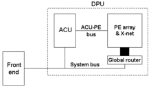
The Array Control Unit (ACU) handles instruction fetch. It is a load-store architecture. The MasPar architecture is Harvard in a broad sense. The ACU implements a microcoded instruction fetch, but achieves a RISC-like 1 instruction per clock. The Arithmetic units, ALUs with data fetch capability, are implemented 32 to a chip. Each ALU is connected in a nearest neighbor fashion to 8 others. The edge connections are brought off-chip. In this scheme, the perimeters can be toroid-wrapped. Up to 16,384 units can be connected within the confines of a cabinet. A global router, essentially a cross-bar switch, provides external I/O to the processor array.

The MP-2 PE chip contains 32 processor elements, each a full 32-bit ALU with floating point, registers, and a barrel shifter. Only the instruction fetch feature is removed, and placed in the ACU. The PE design is literally replicated 32 times on the chip. The chip is designed to interface to DRAM, to other processor array chips, and to communication router chips.
Each ALU, called a PE slice, contains sixty four 32 bit registers that are used for both integer and floating point. The registers are, interestingly, bit and byte addressable. The floating point unit handles single precision and double precision arithmetic on IEEE format numbers. Each PE slice contains two registers for data memory address, and the data. Each PE also has two one-bit serial ports, one for inbound and one for outbound communication to its nearest neighbor. The direction of communication is controlled globally. The PEs also have inbound and outbound paths to a global router for I/O. A broadcast port allows a single instance of data to be "promoted" to parallel data. Alternately, global data can be 'or-ed' to a scalar result.
The serial links support 1 Mbyte/s bit-serial communication that allows coordinated register-register communication between processors. Each processor has its own local memory, implemented in DRAM. No internal memory is included on the processors. Microcoded instruction decode is used.

The 32 PEs on a chip are clustered into two groups sharing a common memory interface, or M-machine, for access. A global scoreboard keeps track of memory and register usage. The path to memory is 16 bits wide. Both big and little endian formats are supported. Each processor has its own 64 Kbyte of memory. Both direct and indirect data memory addressing are supported.
The chip is implemented in 1.0-micrometre, two-level, metal CMOS, dissipates 0.8 watt, and is packaged in a 208-pin PQFP. A relatively low clock rate of 12.5 MHz is used.
The Maspar machines are front ended by a host machine, usually a VAX. They are accessed by extensions to Fortran and C. Full IEEE single- and double-precision floating point are supported.
There is no cache for the ALUs. Cache is not required, due to the memory interface operating at commensurate speed with the ALU data accesses.
The ALUs do not implement memory management for data memory. The ACU uses demand paged virtual memory for the instruction memory.
See also
References
- ↑ Bloomberg Businessweek, Company Overview of Neovista Software, Inc.
- ↑ DSstar Vol. 5 No. 27 (July 3, 2001), JDA Software Buys Accrue Software's NeoVista DM Products