Inelastic electron tunneling spectroscopy

Left: Traveling electrons do not have sufficient energy to excite a vibration. Only elastic tunneling can take place.
Middle: When increasing the bias voltage beyond V=E/e (where e is the electronic charge), traveling electrons do have sufficient energy to excite a vibration with energy E. Inelastic tunneling can take place.
Right: Traveling electrons can also excite and subsequently reabsorb a vibration, which leads to second order elastic tunneling.
Inelastic electron tunneling spectroscopy (IETS) is an experimental tool for studying the vibrations of molecular adsorbates on metal oxides. It yields vibrational spectra of the adsorbates with high resolution (< 0.5 meV) and high sensitivity (< 1013 molecules are required to provide a spectrum).[1] An additional advantage is the fact that optically forbidden transitions may be observed as well.[2] Within IETS, an oxide layer with molecules adsorbed on it is put between two metal plates. A bias voltage is applied between the two contacts. An energy diagram of the metal-oxide-metal device under bias is shown in the top figure. The metal contacts are characterized by a constant density of states, filled up to the Fermi energy. The metals are assumed to be equal. The adsorbates are situated on the oxide material. They are represented by a single bridge electronic level, which is the upper dashed line. If the insulator is thin enough, there is a finite probability that the incident electron tunnels through the barrier. Since the energy of the electron is not changed by this process, it is an elastic process. This is shown in the left figure.
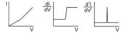
Some of the tunneling electrons can lose energy by exciting vibrations of the oxide or the adsorbate. These inelastic processes lead to a second tunneling path, which gives an additional current contribution to the tunneling current. Since the incident electron should have enough energy to excite this vibration, there is a minimum energy that is the onset of this (inelastic) process. This is shown in the middle figure, where the lower dashed line is a vibronic state. This minimum energy for the electron corresponds with a minimum bias voltage, which is the onset for the additional contribution. The inelastic contribution to the current is small compared to the elastic tunneling current (~0.1%) and is more clearly seen as a peak in the second derivative of the current to the bias voltage, as can be seen in the bottom figure.
There is however also an important correction to the elastic component of the tunneling current at the onset. This is a second order effect in electron-vibration coupling, where a vibration is emitted and reabsorbed or vice versa. This is shown in the upper figure on the right. Depending on the energetic parameters of the system, this correction may be negative and it may outweigh the positive contribution of the inelastic current, resulting in a dip in the IETS spectrum. This is experimentally verified in both regular IETS[3] and in STM-IETS[4] and is also predicted theoretically.[5] Not only peaks and dips may be observed, but depending on the energetic parameters also derivative-like features may be observed, both experimentally[6] and theoretically.[7]
STM-IETS
Keeping the tip of a scanning tunneling microscope (STM) at fixed position over the surface and sweeping the bias voltage, one can record a I-V characteristic. This technique is called scanning tunneling spectroscopy (STS). The first derivative gives information about the local density of states (LDOS) of the substrate, assuming that the tip has a constant density of states. The second derivative gives information on vibrations of the adsorbate as in IETS, which is why this technique is commonly called STM-IETS. In this case the role of the insulating oxide layer is played by the gap between the tip and the adsorbate.
STM-IETS was first demonstrated by Stipe, Rezaei and Ho in 1998, seventeen years after the development of the STM.[8] The requirements of cryogenic temperatures and extreme mechanical stability (mechanical vibrations of the tip over the adsorbate must have amplitudes in the range of picometers or less) make this technique experimentally challenging to realize.
In recent years molecular transport junctions have been produced with one single molecule between two electrodes, sometimes with an additional, gate electrode near the molecule.[9][10][11] The advantage of this method in comparison with STM-IETS is that there is contact between both electrodes and the adsorbate, whereas in STM-IETS there is always a tunneling gap between the tip and the adsorbate. The disadvantage of this method is that it is experimentally very challenging to create and identify a junction with exactly one molecule between the electrodes.
References
- ↑ Langan, J; Hansma, P (1975). "Can the concentration of surface species be measured with inelastic electron tunneling?☆". Surface Science. 52: 211. Bibcode:1975SurSc..52..211L. doi:10.1016/0039-6028(75)90020-5.
- ↑ K.W. Hipps and U. Mazur (2001) Inelastic Electron Tunneling Spectroscopy, Handbook of Vibrational Spectroscopy, ISBN 978-0-471-98847-2
- ↑ Bayman, A.; Hansma, P.; Kaska, W. (1981). "Shifts and dips in inelastic-electron-tunneling spectra due to the tunnel-junction environment". Physical Review B. 24 (5): 2449. Bibcode:1981PhRvB..24.2449B. doi:10.1103/PhysRevB.24.2449.
- ↑ Hahn, J.; Lee, H.; Ho, W. (2000). "Electronic Resonance and Symmetry in Single-Molecule Inelastic Electron Tunneling". Physical Review Letters. 85 (9): 1914–7. Bibcode:2000PhRvL..85.1914H. doi:10.1103/PhysRevLett.85.1914. PMID 10970646.
- ↑ Persson, B.; Baratoff, A. (1987). "Inelastic electron tunneling from a metal tip: the contribution from resonant processes". Physical Review Letters. 59 (3): 339–342. Bibcode:1987PhRvL..59..339P. doi:10.1103/PhysRevLett.59.339. PMID 10035735.
- ↑ Wang, Wenyong; Lee, Takhee; Kretzschmar, Ilona; Reed, Mark A. (2004). "Inelastic Electron Tunneling Spectroscopy of an Alkanedithiol Self-Assembled Monolayer". Nano Letters. 4 (4): 643. Bibcode:2004NanoL...4..643W. doi:10.1021/nl049870v.
- ↑ Mii, Takashi; Tikhodeev, Sergei; Ueba, Hiromu (2003). "Spectral features of inelastic electron transport via a localized state". Physical Review B. 68 (20): 205406. Bibcode:2003PhRvB..68t5406M. doi:10.1103/PhysRevB.68.205406.
- ↑ Stipe, B. C.; Rezaei, M. A.; Ho, W. (1998). "Single-Molecule Vibrational Spectroscopy and Microscopy". Science. 280 (5370): 1732–1735. doi:10.1126/science.280.5370.1732. PMID 9624046. Retrieved 27 September 2013.
- ↑ Smit, R. H. M.; Noat, Y.; Untiedt, C.; Lang, N. D.; Van Hemert, M. C.; Van Ruitenbeek, J. M. (2002). "Measurement of the conductance of a hydrogen molecule". Nature. 419 (6910): 906–9. arXiv:cond-mat/0208407
 . Bibcode:2002Natur.419..906S. doi:10.1038/nature01103. PMID 12410305.
 - ↑ Park, Jiwoong; Pasupathy, Abhay N.; Goldsmith, Jonas I.; Chang, Connie; Yaish, Yuval; Petta, Jason R.; Rinkoski, Marie; Sethna, James P.; et al. (2002). "Coulomb blockade and the Kondo effect in single-atom transistors". Nature. 417 (6890): 722–5. Bibcode:2002Natur.417..722P. doi:10.1038/nature00791. PMID 12066179.
- ↑ Liang, Wenjie; Shores, Matthew P.; Bockrath, Marc; Long, Jeffrey R.; Park, Hongkun (2002). "Kondo resonance in a single-molecule transistor". Nature. 417 (6890): 725–9. Bibcode:2002Natur.417..725L. doi:10.1038/nature00790. PMID 12066180.