IC power-supply pin
Almost all integrated circuits (ICs) have at least two pins that connect to the power rails of the circuit in which they are installed. These are known as the power-supply pins. However, the labeling of the pins varies by IC family and manufacturer.
| Typical supply pin labeling | ||||
|---|---|---|---|---|
| BJT | FET | |||
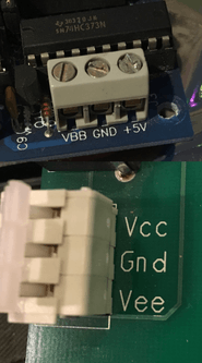
| VCC | VDD | V+ | VS+ | Positive supply voltage |
| VEE | VSS | V− | VS− | Negative supply voltage |
The simplest labels are V+ and V−, but internal design and historical traditions have led to a variety of other labels being used. V+ and V− may also refer to the non-inverting (+) and inverting (−) voltage inputs of ICs like op amps.
Sometimes one of the power-supply pins will be referred to as ground (abbreviated "GND"). In digital logic, this is nearly always the negative pin; in analog integrated circuits, it is most likely to be a pin intermediate in voltage between the most positive and most negative pins .
While double subscript notation, where subscripted letters denote the difference between two points, uses similar looking placeholders with subscripts, the double letter supply voltage subscript notation is not directly linked (though it may have been an influencing factor)[1][2]
History
In circuit diagrams and circuit analysis, there are long-standing conventions regarding the naming of voltages, currents, and some components.[3] In the analysis of a bipolar junction transistor, for example in a common emitter configuration, the DC voltage at the collector, emitter, and base (with respect to ground) may be written as VC , VE , and VB , respectively. Resistors associated with these transistor terminals may be designated RC , RE , and RB . In order to create the DC voltages, the furthest voltage, beyond these resistors or other components if present, was often referred to as VCC , VEE , and VBB . In practice VCC and VEE then refer to the plus and minus supply lines respectively in common NPN circuits. Note that VCC would be negative and VEE would be positive in equivalent PNP circuits.
Exactly analogous conventions were applied to field-effect transistors with their drain, source and gate terminals.[3] This led to VD and VS being created by supply voltages designated VDD and VSS in the more common circuit configurations. In equivalence to the difference between NPN and PNP bipolars, VDD is positive with regard to VSS in the case of n-channel FETs and MOSFETs and negative for circuits based on p-channel FETs and MOSFETs.
Although still in relatively common use, there is limited relevance of these device-specific power supply designations in circuits that use a mixture of bipolar and FET elements, or in those that employ either both NPN and PNP transistors or both n- and p-channel FETs. This latter case is very common in modern chips, which are often based on CMOS technology, where the C stands for complementary meaning that complementary pairs of n- and p-channel devices are common throughout.
These naming conventions were part of a bigger picture where, to continue with bipolar transistor examples although the FET remains entirely analogous, DC or bias currents into or out of each terminal may be written IC , IE , and IB . Apart from DC or bias conditions, many transistor circuits also process a smaller audio-, video-, or radio-frequency signal that is superimposed on the bias at the terminals. Lower case letters and subscripts are used to refer to these signal levels at the terminals, either peak-to-peak or RMS as required. So we see vc , ve , and vb , as well as ic , ie , and ib . Using these conventions, in a common emitter amplifier, the ratio vc/vb represents the small-signal voltage gain at the transistor and vc/ib the small-signal trans-resistance from which the name transistor is derived by contraction. In this convention, vi and vo usually refer to the external input and output voltages of the circuit or stage.[3]
Similar conventions were applied to circuits involving vacuum tubes or thermionic valves as they were known outside of the U.S. Therefore, we see VP , VK , and VG referring to plate (or anode outside of the U.S.), cathode (note K, not C) and grid voltages in analyses of vacuum triode, tetrode, and pentode circuits.[3]
Modern use
CMOS ICs have generally borrowed the NMOS convention of VDD for positive and VSS for negative even though both positive and negative supply rails connect to source terminals (the positive supply goes to PMOS sources, the negative supply to NMOS sources). ICs using bipolar transistors have VCC (positive) and VEE (negative) power supply pins.
In many single supply digital and analog circuits the negative power supply is also called "GND". In "split rail" supply systems there are multiple supply voltages. Examples of such systems include modern cell phones, with GND and voltages such as 1.2 V, 1.8 V, 2.4 V, 3.3 V and PCs, with GND and voltages such as −5 V, 3.3 V, 5 V, 12 V. Power-sensitive designs often have multiple power rails at a given voltage, using them to conserve energy by switching off supplies to components which are not in active use.
More advanced circuits will often have pins carrying voltage levels for more specialized functions and these are generally labeled with some abbreviation of their purpose. For example, VUSB for the supply delivered to a USB device (nominally 5 V), VBAT for a battery, or Vref for the reference voltage for an analog-to-digital converter. Systems combining both digital and analog circuits often distinguish digital and analog grounds (GND and AGND), helping isolate digital noise from sensitive analog circuits. High-security cryptographic devices and other secure systems sometimes require separate power supplies for their unencrypted and encrypted (red/black) subsystems to prevent leakage of sensitive plaintext.
See also
- 4000 series
- 7400 series
- Bob Widlar
- Differential amplifier
- List of 4000 series integrated circuits
- List of 7400 series integrated circuits
- Logic family
- Logic gate
- Open collector
- Operational amplifier applications
- Pin-compatibility
References
- ↑ Micro E, 7. Integrated circuits
- ↑ Washington and Lee University, Lexington, VA, Op-amps: Some Standard Conconfigurations and Applications, Fall 2012
- 1 2 3 4 Alley, Charles L; Atwood, Kenneth W (1973). Electronic Engineering (Third ed.). New York and London: John Wiley & Sons, Inc. ISBN 0-471-02450-3.