hyperSPARC
| Produced | From 1993 to 1996 |
|---|---|
| Designed by | Ross Technology |
| Max. CPU clock rate | 40 MHz to 200 MHz |
| Instruction set | SPARC V8 |
| Cores | 1 |
The hyperSPARC, code-named "Pinnacle", is a microprocessor that implements the SPARC Version 8 instruction set architecture (ISA) developed by Ross Technology for Cypress Semiconductor.
The hyperSPARC was introduced in 1993, and competed with the Sun Microsystems SuperSPARC. Raju Vegesna was the microarchitect. The hyperSPARC was Sun Microsystem's primary competitor in the mid-1990s. When Fujitsu acquired Ross from Cypress, the hyperSPARC was considered to be more important by its new owner than the SPARC64 developed by HAL Computer Systems, also a Fujitsu subsidiary, a view which was shared with analysts.
Description
The hyperSPARC was a two-way superscalar microprocessor. It had four execution units: an integer unit, a floating-point unit, a load/store unit and a branch unit. The hyperSPARC has an on-die 8 KB instruction cache, from which two instructions were fetched per cycle and decoded. The decoder could not decode new instructions if the previously decoded instructions were not issued to the execution units.
The integer register file contained 136 registers, providing eight register windows, a feature defined in the SPARC ISA. It had two read ports. The integer unit had a four-stage pipeline, of which two stages were added so the pipeline would be equal to all non-floating-point pipelines. Integer multiply and divide, instructions added in the V8 version of the SPARC architecture, had an 18- and 37-cycle latency, respectively, and stalled the pipeline until they were completed.
The microprocessor supported multiprocessing on MBus systems.
Physical
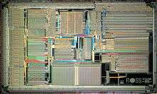
The hyperSPARC consists of 1.2 million transistors. It was fabricated by Cypress in their 0.65 µm, two-layer metal, complementary metal–oxide–semiconductor (CMOS) process. Later iterations of the hyperSPARC have more transistors due to new features, and were ported to newer processes. They were fabricated by Fujitsu, except for the last iteration, which was fabricated by NEC.
Packaging
The hyperSPARC was a multi-chip design. It was packaged in a ceramic multi-chip module (MCM) with a pin grid array (PGA).
Chipsets
The hyperSPARC used the Cypress SparcSet chipset which was introduced in late July 1992. It was developed by Santa Clara, California start-up Nimbus Technologies, Inc. for Cypress, who fabricated the design. SparcSet was also compatible with other SPARC microprocessors.
References
- Levine, Bernard (11 April 1994). "MCM advocates lure would-be users". Electronic News.
- Holden, Daniel (15 February 1993). "Cypress, Sun: HyperSPARC hypertension". Electronic News.
- Holden, Daniel (15 March 1993). "HyperSparc eyes union with Intel on P6 processor". Electronic News.
- Holden, Daniel (19 April 1993). "HyperSPARC slow going with Sun Micro". Electronic News.
- Shen, John Paul and Lipasti, Mikko H. (2004). Modern Processor Design. McGraw-Hill Professional.
Further reading
- "Ross Previews Pinnacle SPARC Design". (25 March 1992). Microprocessor Report, vol. 6, no. 4.
- "TI and Cypress/Ross Battle for SPARC Leadership". (27 May 1992). Microprocessor Report, vol. 6, no. 7.
- "Ross Finally Ships HyperSPARC". (15 November 1993). Microprocessor Report, vol. 7, no. 15.
- "Enhanced HyperSparc Challenges UltraSparc". (4 December 1995). Microprocessor Report, vol. 9, no. 16.