Emotion Engine
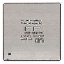
The Emotion Engine is a central processing unit developed and manufactured by Sony Computer Entertainment and Toshiba for use in the PlayStation 2 video game console. It was also used in early PlayStation 3 models sold in Japan and North America (Model Numbers CECHAxx & CECHBxx), to provide PlayStation 2 game support. Mass production of the Emotion Engine began in 1999 and ended in late 2012 with the discontinuation of the PlayStation 2.[1]
Description
The Emotion Engine consists of eight separate "units", each performing a specific task, integrated onto the same die. These units are: a CPU core, two Vector Processing Units (VPU), a 10 channel DMA unit, a memory controller, and an Image Processing Unit (IPU). There are three interfaces: an input output interface to the I/O processor, a graphics interface (GIF) to the graphics synthesizer, and a memory interface to the system memory.[2]
The CPU core is tightly coupled to the first VPU, VPU0. Together, they are responsible for executing game code and high-level modeling computations. The second VPU, VPU1, is dedicated to geometry-transformations and lighting and operates independently, parallel to the CPU core, controlled by microcode. VPU0, when not utilized, can also be used for geometry-transformations. Display lists generated by CPU/VPU0 and VPU1 are sent to the GIF, which prioritizes them before dispatching them to the Graphics Synthesizer for rendering.
CPU core
The CPU core is a two-way superscalar in-order RISC processor. Based on the MIPS R5900, it implements the MIPS-III instruction set architecture (ISA) and much of MIPS-IV, in addition to a custom instruction set developed by Sony which operated on 128-bit wide groups of either 32-bit, 16-bit, or 8-bit integers in single instruction multiple data (SIMD) fashion (i.e. four 32-bit integers could be added to four others using a single instruction). Instructions defined include: add, subtract, multiply, divide, min/max, shift, logical, leading-zero count, 128-bit load/store and 256-bit to 128-bit funnel shift in addition to some not described by Sony for competitive reasons. Contrary to some misconceptions, these SIMD capabilities did not amount to the processor being "128-bit", as neither the memory addresses nor the integers themselves were 128-bit, only the shared SIMD/integer registers. For comparison, 128-bit wide registers and SIMD instructions had been present in the 32-bit x86 architecture since 1999, with the introduction of SSE. However the internal data paths were 128bit wide, and its processors were capable of operating on 4x32bit quantities in parallel in single registers.
The processor is MIPS-based modified instructions, the main VU0 core is a superscalar, in-order 2-issue design with 6 stage long integer pipelines and 15 stage long floating point pipeline, 32 entries 128 bit VLIW SIMD registers(naming/renaming), one 64 bit accumulator and two entries 64 bit general data register, 8 entries 16 bit fix function registers and 16 entries 8 bit controller registers, two 64 bit integer ALUs, 128bit Load-Store Unit(LSU), Branch Execution Unit(BXU) and a 32 bit VU1 FPU coprocessor(acted as sync controller for VPU0/VPU1 ) that contain a MIPS base processor core with 32 entries 64bit FP registers and 15 entries 32bit integer registers. ALUs are 64-bit but FPU is 32-bit and isn't IEEE 754 compliant. The custom instruction set 107 MMI(Multimedia Extensions) was implemented by grouping the two 64-bit integer ALUs. Both the integer and floating-point pipelines are six stages long.
To feed the execution units with instructions and data, there is a 16 KB two-way set associative instruction cache, an 8 KB[3] two-way set associative non blocking data cache and a 16 KB scratchpad RAM. Both the instruction and data caches are virtually indexed and physically tagged while the scratchpad RAM exists in a separate memory space. A combined 48 double entry instruction and data translation lookaside buffer is provided for translating virtual addresses. Branch prediction is achieved by a 64-entry branch target address cache and a branch history table that is integrated into the instruction cache. The branch mispredict penalty is three cycles due to the short six stage pipeline.
Vector processing units
The majority of the Emotion Engine's floating point performance is provided by two vector processing units (VPU), designated VPU0 and VPU1. These were essentially DSPs tailored for 3D maths, and the forerunner to hardware vertex shader pipelines. Each VPU features 32 128-bit vector SIMD registers (holding 4D vector data), 16 16-bit fixed-point registers, four FMAC (Floating point Multiply-ACcumulate) units, a FDIV (Floating point DIVide) unit and a local data memory. The data memory for VPU0 is 4 KB in size, while VPU1 features a 16 KB data memory.
To achieve high bandwidth, the VPU's data memory is connected directly to the GIF, and both of the data memories can be read directly by the DMA unit. A single vector instruction consists of four 32-bit single-precision floating-point values which are distributed to the four single-precision (32-bit) FMAC units for processing. Contrary to popular belief, the Emotion Engine is not a 128-bit processor as it does not process a single 128-bit value, but a group of four 32-bit values that are stored in one 128-bit register.[4][5] This scheme is similar to the SSEx extensions by Intel.
The FMAC units take four cycles to execute one instruction, but as the units have a six-stage pipeline, they have a throughput of one instruction per cycle. The FDIV unit has a nine-stage pipeline and can execute one instruction every seven cycles.
Image Processing Unit (IPU)
The IPU allowed MPEG-2 compressed image decoding, allowing playback of DVDs and game FMV. It also allowed vector quantization for 2D graphics data.[6]
DMA, DRAM and Memory Management Unit (MMU)
The memory management unit, RDRAM controller and DMA controller handle memory access within the system.[6]
Internal data bus
Communications between the MIPS core, the two VPUs, GIF, memory controller and other units is handled by a 128-bit wide internal data bus running at half the clock frequency of the Emotion Engine but, to offer greater bandwidth, there is also a 128-bit dedicated path between the CPU and VPU0 and a 128-bit dedicated path between VPU1 and GIF. At 150 MHz, the internal data bus provides a maximum theoretical bandwidth of 2.4 GB/s.
External interface
Communication between the Emotion Engine and RAM occurs through two channels of DRDRAM (Direct Rambus Dynamic Random Access Memory) and the memory controller, which interfaces to the internal data bus. Each channel is 16 bits wide and operates at 400 MHz DDR (Double Data Rate). Combined, the two channels of DRDRAM have a maximum theoretical bandwidth of 25.6 Gbit/s (3.2 GB/s), about 33% more bandwidth than the internal data bus. Because of this, the memory controller buffers data sent from the DRDRAM channels so the extra bandwidth can be utilised by the CPU.
The Emotion Engine interfaces directly to the Graphics Synthesizer via the GIF with a dedicated 64-bit, 150 MHz bus that has a maximum theoretical bandwidth of 1.2 GB/s.[7]
To provide communications between the Emotion Engine and the Input Output Processor (IOP), the input output interface interfaces a 32-bit wide, 37.5 MHz input output bus with a maximum theoretical bandwidth of 150 MB/s to the internal data bus. This interface provides vastly more bandwidth than what is required by the PlayStation's input output devices.
Fabrication
The Emotion Engine contained 10.5 million transistors on a die measuring 240 mm2. It was fabricated by Sony and Toshiba in a 0.25 µm (0.18 µm effective LG) complementary metal–oxide–semiconductor (CMOS) process with four levels of interconnect.
Packaging
The Emotion Engine was packaged in a 540-contact plastic ball grid array (PBGA).
Uses
The primary use of the Emotion Engine was to serve as the PlayStation 2's CPU. The first SKUs of the PlayStation 3 also featured an Emotion Engine on the motherboard to achieve backwards compatibility with PlayStation 2 games. However, the second revision of the PlayStation 3 lacked a physical Emotion Engine in order to lower costs, performing all of its functions using software emulation performed by the Cell Broadband Processor, coupled with a hardware Graphics Synthesizer still present to achieve PlayStation 2 backwards compatibility. In all subsequent revisions, the Graphics Synthesizer was removed; however, a PlayStation 2 software emulator is available in later system software revisions for use with Sony's PS2 Classics titles available for purchase on the Sony Entertainment Network.
PlayStation 2 technical specifications
- Clock frequency: 294 MHz, 299 MHz (later versions)
- Instruction set: MIPS III, MIPS IV subset, 107 vector instructions
- 2 issue, 2 64-bit fixed point units, 1 floating point unit, 6 stage pipeline
- Instruction cache: 16 KB, 2-way set associative
- Data cache: 8 KB, 2-way set associative
- Scratchpad RAM: 16 KB
- Translation look aside buffer: 48-entry combined instruction/data
- Vector processing unit: 4 FMAC units, 1 FDIV unit
- Vector processing unit registers: 128-bit wide, 32 entries
- Image processing unit: MPEG2 macroblock layer decoder
- Direct memory access: 10 channels
- VDD Voltage: 1.8 V
- Power consumption: 15 W at 1.8 V
Theoretical performance
- Floating point: 6.2 billion single precision (32-bit) floating point operations per second
- Perspective transformation: 66 million polygons per second
- With lighting and fog: 36 million polygons per second
- Bézier surface patches: 16 million polygons per second
- Image decompression: 150 million pixels per second
Notes
- ↑ Gilbert, Ben. "Sony confirms production end for PlayStation 2 worldwide". Engadget. Retrieved 23 June 2013.
- ↑ "Sound and Vision: A Technical Overview of the Emotion Engine". Ars Technica. 16 Feb 2000. Retrieved 9 June 2015.
- ↑ Transistorized memory, such as RAM, ROM, flash and cache sizes as well as file sizes are specified using binary meanings for K (10241), M (10242), G (10243), ...
- ↑ Hennessy, Patterson 2003, p. ?
- ↑ Diefendorff 1999, p. 3
- 1 2 "The Playstation 2 Linux Kit Handbook". Free Software Foundation, Inc. 2002.
- ↑ Diefendorff 1999, p. 5
See also
- Graphics card
- Graphics processing unit
- Computer graphics
- List of computer graphics and descriptive geometry topics
- Cell microprocessor, a design inspired by the Emotion Engines' CPU+VU0/VU1 arrangement, used in the PlayStation 3
References
- Hennessy, John L.; Patterson, David A. (29 May 2002). Computer Architecture: A Quantitative Approach (3 ed.). Morgan Kaufmann. ISBN 978-0-08-050252-6. Retrieved 9 April 2013.
- Diefendorff, Keith (19 April 1999). "Sony's Emotionally Charged Chip". Microprocessor Report. Microdesign Resources. 13 (5).
External links
- Sound and Vision: A Technical Overview of the Emotion Engine
- The PlayStation2 vs. the PC: a system-level comparison of two 3D platforms
- Scientific Computing on the Sony PlayStation 2
- BBC article: PlayStation turns supercomputer