Current limiting
Current limiting is the practice in electrical or electronic circuits of imposing an upper limit on the current that may be delivered to a load with the purpose of protecting the circuit generating or transmitting the current from harmful effects due to a short-circuit or similar problem in the load.
Inrush current limiting
An inrush current limiter is a device or group of devices used to limit inrush current. Negative temperature coefficient (NTC) thermistors and resistors are two of the simplest options, with cool-down time and power dissipation being their main drawbacks, respectively. More complex solutions can be used when design constraints make simpler options infeasible.
In electronic power circuits
Electronic circuits like regulated DC power supplies and power amplifiers employ, against fuses, active current limiting since a fuse alone may not be able to protect the internal devices of the circuit in an over-current or short-circuit situation. A fuse generally is too slow in operation and the time it takes to blow may well be enough to destroy the devices.
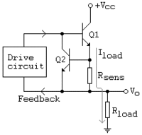
A typical short-circuit/overload protection scheme is shown in the image. The schematic is representative of a simple protection mechanism employed in regulated DC supplies and class-AB power amplifiers.[lower-alpha 1]
Q1 is the pass or output transistor. Rsens is the load current sensing device. Q2 is the protection transistor which turns on as soon as the voltage across Rsens becomes about 0.65 V. This voltage is determined by the value of Rsens and the load current through it (Iload).
When Q2 turns on, it removes base current from Q1 thereby reducing the collector current of Q1. Neglecting the base currents of Q1 and Q2, the collector current of Q1 is also the load current. Thus, Rsens fixes the maximum current to a value given by 0.65/Rsens, for any given output voltage and load resistance.
For example, if Rsens = 0.33 Ω, the current is limited to about 2 A even if Rload becomes a short (and Vo becomes zero). With the absence of Q2, Q1 would attempt to drive a very large current (limited only by Rsens, and dependent on the output voltage Vo if Rload is not zero) and the result would be greater power dissipation in Q1.
If Rload is zero the dissipation will be much greater (enough to destroy Q1). With Q2 in place, the current is limited and the maximum power dissipation in Q1 is also limited to a safe value (though this is also dependent on Vcc, Rload and current-limited Vo).
Further, this power dissipation will remain as long as the overload exists, which means that the devices must be capable of withstanding it for a substantial period. For example, the pass-transistor in a regulated DC power supply system (corresponding to Q1 in the schematic above) rated for 25 V at 1.5 A (with limiting at 2 A) will normally (i.e., with rated load of 1.5 A) dissipate about 7.5 W for a Vcc of 30 V.[lower-alpha 2]
With current limiting, the dissipation will increase to about 60 W if the output is shorted‡‡ (2). Without current limiting the dissipation would be greater than 300 W‡‡ (3) - so limiting does have a benefit, but it turns out that the pass-transistor must now be capable of dissipating at least 60 W.
In short, an 80–100 W device will be needed (for an expected overload and limiting) where a 10–20 W device (with no chance of shorted load) would have been sufficient. In this technique, beyond the current limit the output voltage will decrease to a value depending on the current limit and load resistance.
- ↑ For class-AB stages, the circuit will be mirrored vertically and complementary devices will be used for Q1 & Q2.
- ↑ The following conditions are considered for determining the power dissipation in Q1, with Vo = 25 V, Iload = 1.5 A (limit at 2 A), Rsens = 0.33 Ω (for limiting at 2 A) and Vcc = 30 V —
- Normal operation
- Vo = 25 V at a load current of 1 A. So Q1 dissipates a power of (30 − 25) V × 1.5 A = 7.5 W. The transistor used must be a 10–20 W device to account for ambient temperature (i.e., derated) and must be mounted on a heat-sink.
- Output shorted, with limiting at 2 A
- The dissipation is given by (30 − 0.65) V × 2 A = 58.7 W. The 0.65 V is the drop across Rsens. In practice, if the power supply Vcc is not able to provide the maximum short-circuit current it will collapse thereby reducing dissipation in Q1. However this is dependent on how "stiff" the supply is. A stiffer supply will sustain the voltage for a heavier current draw before collapsing. Further, the transistor used must be an 80–100 W device to account for ambient temperature (i.e., derated) and must be mounted on a heat-sink.
- Output shorted, and no limiting
- A shorted load will mean that only Rsens is present as the load. With this, the circuit will attempt to put 25 V across Rsens (0.33 Ω) - here the output voltage has to be measured at the emitter of Q1 since Q1 is connected as an emitter-follower and the lower end of Rsens is effectively grounded due to the short. Thus the load current (and collector current of Q1) becomes nearly 76 A, and the dissipation in Q1 becomes (30 − 25) V × 76 A = 380 W. This is a very large power to dissipate, since in normal circumstances Q1 will only be required to dissipate about 7.5 W (60 W at worst with limiting), and even a 100 W transistor will not withstand a 380 W dissipation. Without Rsens (i.e., Q1 emitter is directly connected to the load) the situation is even worse — Q1 becomes a dead short across 30 V and will draw current limited only by its internal resistance. In practice, the dissipation will be less because the supply (Vcc) will collapse under such a condition. However the dissipation will still be enough to destroy Q1.
Single power-supply circuits


An issue with the previous circuit is that Q1 will not be saturated unless its base is biased about 0.5 volts above Vcc.
The circuits at right and left operate more efficiently from a single (Vcc) supply. In both circuits, R1 allows Q1 to turn on and pass voltage and current to the load. When the current through R_sense exceeds the design limit, Q2 begins to turn on, which in turn begins to turn off Q1, thus limiting the load current. The optional component R2 protects Q2 in the event of a short-circuited load. When Vcc is at least a few volts, a MOSFET can be used for Q1 for lower dropout voltage. Due to its simplicity, this circuit is sometimes used as a current source for high-power LEDs.[1]
Slew rate control
Many electronics designers put a small resistor on IC output pins.[2] This slows the edge rate which improves electromagnetic compatibility. Some devices have this "slew rate limiting" output resistor built in; some devices[3][4][5][6] have programmable slew rate limiting. This provides overall slew rate control.
See also
- Current source - A type of current limiter
- Crowbar
- Fault current limiter
References
- ↑ "The New Stuff!!! Constant Current Source #1". Instructables. Retrieved 4 July 2012.
- ↑ IC output series resistor
- ↑ Freescale MC9S12XHZ512
- ↑ Microchip PIC18F87J50
- ↑ Initio INIC-940 Archived October 18, 2006, at the Wayback Machine.
- ↑ Fairchild FDC6901L