List of AMD graphics processing units
This page contains general information about the GPUs and video cards by Advanced Micro Devices (AMD), including those by ATI Technologies before 2006, based on official specifications in table form.
Direct3D version note
Direct3D version indicates which graphics acceleration operations the card implements.
- Direct3D 6.0 - Multitexturing
- Direct3D 7.0 - Hardware Transformation, Clipping and Lighting (TCL/T&L)
- Direct3D 8.0 - Pixel Shader 1.1 & Vertex Shader 1.1
- Direct3D 8.1 - Pixel Shader 1.4 & Vertex Shader 1.1
- Direct3D 9.0 - Shader Model 2.0
- Direct3D 9.0b - Pixel Shader 2.0b & Vertex Shader 2.0
- Direct3D 9.0c - Shader Model 3.0, GPGPU
- Direct3D 9.0L - Windows Vista only, Direct3D 9.0c, Shader Model 3.0, Windows Graphics Foundation 1.0, DXVA 1.0, GPGPU
- Direct3D 10.0 - Windows Vista/Windows 7, Shader Model 4.0, Windows Graphics Foundation 2.0, DXVA 2.0, GPGPU
- Direct3D 10.1 - Windows Vista SP1/Windows 7, Shader Model 4.1, Windows Graphics Foundation 2.1, DXVA 2.1, GPGPU
- Direct3D 11.0 - Windows Vista SP2/Windows 7, Shader Model 5.0, Tessellation, Multithreaded rendering, Compute shaders, implemented by hardware and software running Direct3D 9/10/10.1, GPGPU
- Direct3D 11.1 - Windows 7 SP1/Windows 8, Stereoscopic 3D Rendering, GPGPU
- Direct3D 11.2 - Windows 8.1, Tiled resources, GPGPU
- Direct3D 11.3 - Windows 10, Shader Model 5.1, GPGPU
- Direct3D 12.0 - Windows 10, low-level rendering API, GPGPU
OpenGL version note
OpenGL version indicates which graphics acceleration operations the card implements.
- OpenGL 1.1 - Texture objects
- OpenGL 1.2 - 3D textures, BGRA and packed pixel formats[1]
- OpenGL 1.3 - Multitexturing, multisampling, texture compression
- OpenGL 1.4 - Depth textures
- OpenGL 1.5 - Vertex Buffer Object (VBO), Occlusion Queries[2]
- OpenGL 2.0 - GLSL 1.1, MRT, Non Power of Two textures, Point Sprites, Two-sided stencil[2]
- OpenGL 2.1 - GLSL 1.2, Pixel Buffer Object (PBO), sRGB Textures[2]
- OpenGL 3.0 - GLSL 1.3, Texture Arrays, Conditional rendering, Frame Buffer Object (FBO)[3]
- OpenGL 3.1 - GLSL 1.4, Instancing, Texture Buffer Object, Uniform Buffer Object, Primitive restart [4]
- OpenGL 3.2 - GLSL 1.5, Geometry Shader, Multi-sampled textures [5]
- OpenGL 3.3 - GLSL 3.30 Backports as much function as possible from the OpenGL 4.0 specification
- OpenGL 4.0 - GLSL 4.00 Tessellation on GPU, shaders with 64-bit precision,[6]
- OpenGL 4.1 - GLSL 4.10 Developer-friendly debug outputs, compatibility with OpenGL ES 2.0,[7]
- OpenGL 4.2 - GLSL 4.20 Shaders with atomic counters, draw transform feedback instanced, shader packing, performance improvements
- OpenGL 4.3 - GLSL 4.30 Compute shaders leveraging GPU parallelism, shader storage buffer objects, high-quality ETC2/EAC texture compression, increased memory security, a multi-application robustness extension, compatibility with OpenGL ES 3.0,[8]
- OpenGL 4.4 - GLSL 4.40 Buffer Placement Control, Efficient Asynchronous Queries, Shader Variable Layout, Efficient Multiple Object Binding, Streamlined Porting of Direct3D applications, Bindless Texture Extension, Sparse Texture Extension,[9]
- OpenGL 4.5 - GLSL 4.50 Direct State Access (DSA), Flush Control, Robustness, OpenGL ES 3.1 API and shader compatibility, DX11 emulation features
Video codec acceleration
- R100 - Video Immersion
- R200 - Video Immersion II
- R300 - Video Immersion II + Video Shader
- R410 - Video Shader HD
- R420 - Video Shader HD + DXVA
- R520 - Avivo Video
- R600 - Avivo HD Video - UVD 1.0
- R700 - UVD 2, UVD 2.2
- Evergreen - UVD 2.2
- Northern Islands - UVD 3 (HD 67xx UVD 2.2)
- Southern Islands - UVD 3.1, Video Coding Engine 1.0
- Sea Islands - UVD 4.2, VCE 2.0 [10]
- Volcanic Islands - UVD 5.0, 6.0, Video Coding Engine 3.0[11][12]
- Arctic Islands - UVD 6.3, VCE 3.4
Field explanations
The fields in the table listed below describe the following:
- Model – The marketing name for the processor assigned by ATi. Note that the ATi trademark has been replaced by AMD trademark starting with the Radeon HD 6000 series graphics processing units. Professional graphics processing units will switch to the AMD trademark as well.[13]
- Launch – Date of release for the processor.
- Model number – Mobility VPUs are based on technology from several technology families. ATi assigns codenames based on an "MXX" model string, which does not relate to the actual technological base of the processor (represented by the R-number). Additionally, ATi is the sole supplier for all Mobility Radeon parts. For this reason, except for the Mobility Radeon 2000 series, all Mobility processors are listed on the same table.
- Code name – The internal engineering codename for the processor (typically designated by an RNXX name where N is the series number and XX is the market segment for which the product is designed. Additionally, a codename may follow the RVNXX format where "V" typically signifies a processor intended for a mainstream or value market segment).
- Fab – Fabrication process. Average feature size of components of the processor.
- Bus interface – Bus by which the graphics processor is attached to the system (typically an expansion slot, such as PCI, AGP, or PCIe).
- Memory – The reference amount of memory used by the processor.
- Core clock – The reference core clock frequency (used as some manufacturers adjust clocks lower and higher, this number will always be that listed by ATi).
- Memory clock – The reference memory clock frequency (used as some manufacturers adjust clocks lower and higher, this number will always be that listed by ATi).
- Core config – The layout of the graphics pipeline, in terms of functional units. Over time the number, type and variety of functional units in the GPU core has changed significantly; before each section in the list there is an explanation as to what functional units are present in each generation of processors.
- Performance subsection
- Shader operations - How many operations the pixel shaders (or unified shaders in Direct3D 10 and newer GPUs) can perform. Measured in MOperations/s or GOperations/s.
- Pixel fillrate - The number of pixels the raster operators can render to a display in one second. Measured in MPixels/s or GPixels/s.
- Texture fillrate - The rate at which a texture can be mapped by the texture mapping units onto a polygon mesh in one second. Measured in MTextels/s or GTextels/s.
- Vertex operations - The amount of geometry operations that can be processed on the vertex shaders in one second (only applies to Direct3D 9.0c and older GPUs). Measured in MVertices/s.
- Memory subsection
- Bandwidth – Maximum theoretical bandwidth for the processor at factory clock with factory bus width. GB=109 bytes.
- Bus type – Type of memory bus or buses utilized.
- Bus width – Maximum bit width of the memory bus or buses utilized. This will always be a factory bus width.
- API compliance section
- Direct3D – Highest version of Direct3D with which the hardware is fully compliant.
- OpenGL – Highest version of OpenGL with which the hardware is fully compliant.
- Features – Additional features that are not standard as a part of the two graphics libraries.
Comparison table: Desktop GPUs
Wonder Series
| Model | Launch | Fab (µm) | Bus interface | Core config1 | Memory | API compliance | ||
|---|---|---|---|---|---|---|---|---|
| Size (KiB) | Bus type | Bus width (bit) | ||||||
| Wonder MDA/CGA | 1986 | 1 | PC/XT | 1:1 | 64 | SRAM | 8 | 2D |
| Wonder EGA | 1987 | 1 | PC/XT | 1:1 | 256 | SRAM | 8 | 2D |
| Wonder VGA | 1987 | 1, 0.8 | PC/XT, ISA | 1:1 | 256, 512 1024 |
DRAM | 8, 16 | 2D |
1 Pixel pipelines : Render output units
Mach Series
| Model | Launch | Fab (µm) | Bus interface | Core config1 | Memory | API compliance | ||
|---|---|---|---|---|---|---|---|---|
| Size (KiB) | Bus type | Bus width (bit) | ||||||
| Mach 8 | 1991 | 0.8 | ISA, MCA | 1:1 | 512 1024 |
DRAM VRAM |
32 | 2D |
| Mach 32 | 1992 | 0.8 | ISA, EISA, VLB PCI, MCA |
1:1 | 1024 2048 |
DRAM VRAM |
64 | 2D |
| Mach 64 | 1994 | 0.6 | ISA, VLB, PCI | 1:1 | 1024, 2048, 4096, 8192 | DRAM, VRAM, SGRAM | 64 | 2D |
1 Pixel pipelines : Render output units
Rage Series
| Model | Launch | Fab (nm) | Bus interface | Core clock (MHz) | Memory clock (MHz) | Core config1 | Fillrate | Memory | API compliance | |||||||
|---|---|---|---|---|---|---|---|---|---|---|---|---|---|---|---|---|
| MOperations/s | MPixels/s | MTexels/s | MVertices/s | Size (MiB) | Bandwidth (GB/s) | Bus type | Bus width (bit) | Direct3D | OpenGL | |||||||
| 3D Rage | April 1996[14] | 500 | PCI | 40 | 40 | 1:0:1:1 | 40 | 40 | 40 | 0 | 2 | 0.32 | EDO | 64 | 5.0 | None2 |
| 3D Rage II | September 1996 | 500 | PCI | 60 | 83 | 1:0:1:1 | 60 | 60 | 60 | 0 | 2, 4, 8 | 0.664 | SDR | 64 | 5.0 | None2 |
| Rage Pro | March 1997 | 350 | AGP 2x | 75 | 75 | 1:0:1:1 | 75 | 75 | 75 | 0 | 8, 16 | 0.6 | SDR | 64 | 6.0 | 1.1 |
| Rage XL[15][16][17] | August 1998 | 350 | AGP 2x, PCI | 125 | 83 | 1:0:1:1 | ca. 125 | 125 | 125 | 0 | 8 | 0.664 | SDR | 64 | 6.0 | 1.2 |
| Rage 128 VR | August 1998 | 250 | AGP 2x, PCI | 80 | 120 | 2:0:2:2 | 160 | 160 | 160 | 0 | 8, 32 | 0.96 | SDR | 64 | 6.0 | 1.2 |
| Rage 128 GL | August 1998 | 250 | AGP 2x, PCI | 103 | 103 | 2:0:2:2 | 206 | 206 | 206 | 0 | 32 | 1.648 | SDR | 128 | 6.0 | 1.2 |
| Rage 128 Pro | August 1999 | 250 | AGP 4x, PCI | 125 | 143 | 2:0:2:2 | 250 | 250 | 250 | 0 | 16, 32 | 2.288 | SDR | 128 | 6.0 | 1.2 |
| Rage 128 Ultra | August 1999 | 250 | AGP 4x, PCI | 130 | 130 | 2:0:2:2 | 260 | 260 | 260 | 0 | 16, 32, 64 | 2.088 | SDR | 128 | 6.0 | 1.2 |
| Rage Fury MAXX | October 1999 | 250 | AGP 4x, PCI | 125 | 143 | 2:0:2:2 x2 | 500 | 500 | 500 | 0 | 32 | 4.576 | SDR | 128 x2 | 6.0 | 1.2 |
1 Pixel pipelines : Vertex shaders : Texture mapping units : Render output units
2 OpenGL 1.0 (Generic 2D) is provided through software implementations.
Radeon R100 (7xxx) Series
- All models include Direct3D 7.0 and OpenGL 1.3
| Model | Launch | Code name | Fab (nm) | Bus interface | Core clock (MHz) | Memory clock (MHz) | Core config1 | Fillrate | Memory | ||||||
|---|---|---|---|---|---|---|---|---|---|---|---|---|---|---|---|
| MOperations/s | MPixels/s | MTexels/s | MVertices/s | Size (MiB) | Bandwidth (GB/s) | Bus type | Bus width (bit) | ||||||||
| Radeon VE/7000 | Feb 19, 2001 | RV100 (piglet) | 180 | AGP 4x, PCI | 183 | 366 | 1:0:3:1 | 183 | 336 | 549 | 0 | 32, 64 | 2.688 | DDR | 64 |
| Radeon LE/7100 (OEM) | May 1, 2001 | Rage 6 / R100 | 180 | AGP 4x | 150 | 300 | 2:0:6:2 | 296 | 296 | 888 | 37 | 32 | 4.736 | DDR | 128 |
| Radeon SDR/7200 | June 2000 | Rage 6 / R100 | 180 | AGP 4x | 166 | 166 | 2:0:6:2 | 333 | 333 | 996 | 41.5 | 32 | 2.656 | SDR | 128 |
| Radeon DDR/7200 | April 2000 | Rage 6 / R100 | 180 | AGP 4x | 166/183A | 333/366A | 2:0:6:2 | 333/366A | 333/366A | 966/1098A | 41.5/45.75A | 32, 64 | 5.312/5.856A | DDR | 128 |
| Radeon DDR/7500 VIVO | 2001 | Rage 6 / R100 | 180 | AGP 4x, PCI | 166/183B | 333/366B | 2:0:6:2 | 333/366B | 333/366B | 966/1098B | 41.5/45.75B | 64 | 5.312/5.856B | DDR | 128 |
| Radeon DDR/7500 VIVO "SE" | 2001 | Rage 6 / R100 | 180 | AGP 4x, PCI | 200 | 400 | 2:0:6:2 | 400 | 400 | 1200 | 50.0 | 64 | 6.400 | DDR | 128 |
| Radeon 7500 LE | N/A | RV200 (morpheus) | 150 | AGP 4x, PCI | 250 | 350 | 2:0:6:2 | 500 | 500 | 1500 | 62.5 | 32, 64 | 5.600 | DDR | 128 |
| Radeon 7500 | Aug 14, 2001 | RV200 (morpheus) | 150 | AGP 4x, PCI | 290 | 460 | 2:0:6:2 | 580 | 580 | 1740 | 72.5 | 32, 64 | 7.360 | DDR | 128 |
| Model | Launch | Code name | Fab (nm) | Bus interface | Core clock (MHz) | Memory clock (MHz) | Core config1 | MOperations/s | MPixels/s | MTexels/s | MVertices/s | Size (MiB) | Bandwidth (GB/s) | Bus type | Bus width (bit) |
| Fillrate | Memory | ||||||||||||||
1 Pixel shaders : Vertex shaders : Texture mapping units : Render output units
A First number indicates cards with 32MB of memory. Second number indicates cards with 64MB of memory.
B First number indicates OEM cards. Second number indicates Retail cards.
IGP (3xx Series)
- All models are manufactured with a 180 nm fabrication process
- All models include Direct3D 7.0 and OpenGL 1.4
- Based on the Radeon VE
| Model | Launch | Code name | Bus interface | Core clock (MHz) | Memory clock (MHz) | Core config1 | Fillrate | Memory | ||||||
|---|---|---|---|---|---|---|---|---|---|---|---|---|---|---|
| MOperations/s | MPixels/s | MTexels/s | MVertices/s | Size (MiB) | Bandwidth (GB/s) | Bus type | Bus width (bit) | |||||||
| Radeon 320 | May 2002 | A3 | FSB | 160 | 200, 266 | 1:0:3:1 | 160 | 160 | 480 | 0 | Unknown | 1.6, 2.128 | DDR | 64 |
| Radeon 330 | 2002 | RS200L (wilma) | FSB | 150 | 200, 266 | 1:0:3:1 | 150 | 150 | 450 | 0 | Unknown | 1.6, 2.128 | DDR | 64 |
| Radeon 340 | 2002 | RS200 (wilma) | FSB | 183 | 200, 266 | 1:0:3:1 | 183 | 183 | 549 | 0 | Unknown | 1.6, 2.128 | DDR | 64 |
1 Pixel shaders : Vertex shaders : Texture mapping units : Render output units
Radeon R200 (8xxx, 9xxx) Series
- All models are manufactured with a 150 nm fabrication process
- All models include Direct3D 8.1 and OpenGL 1.4
| Model | Launch | Code name | Bus interface | Core clock (MHz) | Memory clock (MHz) | Core config1 | Fillrate | Memory | ||||||
|---|---|---|---|---|---|---|---|---|---|---|---|---|---|---|
| MOperations/s | MPixels/s | MTexels/s | MVertices/s | Size (MiB) | Bandwidth (GB/s) | Bus type | Bus width (bit) | |||||||
| Radeon 8500 | Aug 14, 2001 | R200 (chaplin) | AGP 4x | 275 | 550 | 4:2:8:4 | 1100 | 1100 | 2200 | 137.5 | 64, 128 | 8.8 | DDR | 128 |
| Radeon 8500 LE | Feb 4, 2002 | R200 (chaplin) | AGP 4x | 250 | 500 | 4:2:8:4 | 1000 | 1000 | 2000 | 125 | 64, 128 | 8 | DDR | 128 |
| Radeon 9000 | Aug 1, 2002 | RV250 (iris) | AGP 4x | 200 | 500 | 4:1:4:4 | 800 | 800 | 800 | 50 | 64, 128 | 6.4 | DDR | 128 |
| Radeon 9000 Pro | Aug 1, 2002 | RV250 (iris) | AGP 4x | 275 | 550 | 4:1:4:4 | 1100 | 1100 | 1100 | 68.75 | 64, 128 | 8.8 | DDR | 128 |
| Radeon 9100 | 2003 | R200 (chaplin) | AGP 8x, PCI | 250 | 500 | 4:2:8:4 | 1000 | 1000 | 2000 | 125 | 64, 128 | 8.0 | DDR | 128 |
| Radeon 9200 | Apr 1, 2003 | RV280 (argus) | AGP 8x, PCI | 250 | 400 | 4:1:4:4 | 1000 | 1000 | 1000 | 62.5 | 64, 128, 256 | 6.4 | DDR | 128 |
| Radeon 9200 SE | July 2003 | RV280 (argus) | AGP 8x, PCI | 200 | 333 | 4:1:4:4 | 800 | 800 | 800 | 50 | 64, 128, 256 | 2.67 | DDR | 64 |
| Radeon 9250 | July 2004 | RV280 (argus) | AGP 8x, PCI | 240 | 400 | 4:1:4:4 | 960 | 960 | 960 | 60 | 64, 128, 256 | 6.4 | DDR | 128 |
1 Pixel shaders : Vertex shaders : Texture mapping units : Render output units
IGP (9xxx Series)
- All models are manufactured with a 150 nm fabrication process
- All models include Direct3D 8.1 and OpenGL 1.4
- Based on the Radeon 9200
| Model | Launch | Code name | Bus interface | Core clock (MHz) | Memory clock (MHz) | Core config1 | Fillrate | Memory | ||||||
|---|---|---|---|---|---|---|---|---|---|---|---|---|---|---|
| MOperations/s | MPixels/s | MTexels/s | MVertices/s | Size (MiB) | Bandwidth (GB/s) | Bus type | Bus width (bit) | |||||||
| Radeon 9000 | 2003 | RC350 | FSB | 300 | 400 | 4:1:2:2 | 600 | 600 | 600 | 0 | 16 - 128 | 3.2 | DDR | 64 |
| Radeon 9100 | 2003 | RS300 (superman) | FSB | 300 | 400 | 4:1:2:2 | 600 | 600 | 600 | 0 | 16 - 128 | 6.4 | DDR | 128 |
| Radeon 9100 Pro | May 3, 2004 | RS350 | FSB | 300 | 400 | 4:1:2:2 | 600 | 600 | 600 | 0 | 16 - 128 | 6.4 | DDR | 128 |
1 Pixel shaders : Vertex shaders : Texture mapping units : Render output units
Radeon R300 Series
AGP (9xxx Series)
- All models include Direct3D 9.0 and OpenGL 2.0
| Model | Launch | Code name | Fab (nm) | Bus interface | Core clock (MHz) | Memory clock (MHz) | Core config1 | Fillrate | Memory | ||||||
|---|---|---|---|---|---|---|---|---|---|---|---|---|---|---|---|
| MOperations/s | MPixels/s | MTexels/s | MVertices/s | Size (MiB) | Bandwidth (GB/s) | Bus type | Bus width (bit) | ||||||||
| Radeon 9500 | Oct. 24, 2002 | R300 (khan) | 150 | AGP 8x | 275 | 540 | 4:4:4:8 | 1100 | 2200 | 1100 | 275 | 64, 128 | 8.64 | DDR | 128 |
| Radeon 9500 Pro | Oct. 24, 2002 | R300 (khan) | 150 | AGP 8x | 275 | 540 | 8:4:8:8 | 2200 | 2200 | 2200 | 275 | 128 | 8.64 | DDR | 128 |
| Radeon 9550 | 2004 | RV350 (shivah) | 130 | AGP 8x | 250 | 400 | 4:2:4:4 | 1000 | 1000 | 1000 | 125 | 64, 128, 256 | 6.4 | DDR | 128 |
| Radeon 9550 SE | 2004 | RV350 (shivah) | 130 | AGP 8x | 250 | 400 | 4:2:4:4 | 1000 | 1000 | 1000 | 125 | 64, 128, 256 | 3.2 | DDR | 64 |
| Radeon 9600 | 2003 | RV350 (shivah) | 130 | AGP 8x | 325 | 400 | 4:2:4:4 | 1300 | 1300 | 1300 | 162.5 | 128, 256 | 6.4 | DDR | 128 |
| Radeon 9600 Pro | 2003 | RV350 (shivah) | 130 | AGP 8x | 400 | 600 | 4:2:4:4 | 1600 | 1600 | 1600 | 200 | 128, 256 | 9.6 | DDR | 128 |
| Radeon 9600 SE | 2003 | RV350 (shivah) | 130 | AGP 8x | 325 | 400 | 4:2:4:4 | 1300 | 1300 | 1300 | 162.5 | 64, 128, 256 | 3.2 | DDR | 64 |
| Radeon 9600 XT | Sept. 30, 2003 | RV360 | 130 | AGP 8x | 500 | 600 | 4:2:4:4 | 2000 | 2000 | 2000 | 250 | 128, 256 | 9.6 | DDR | 128 |
| Radeon 9700 | Oct. 24, 2002 | R300 (khan) | 150 | AGP 8x | 275 | 540 | 8:4:8:8 | 2000 | 2000 | 2000 | 275 | 128 | 17.28 | DDR | 256 |
| Radeon 9700 Pro | July 18, 2002 | R300 (khan) | 150 | AGP 8x | 325 | 620 | 8:4:8:8 | 2600 | 2600 | 2600 | 325 | 128 | 19.84 | DDR | 256 |
| Radeon 9800 | 2003 | R350 | 150 | AGP 8x | 325 | 620 | 8:4:8:8 | 2600 | 2600 | 2600 | 325 | 128 | 19.84 | DDR | 256 |
| Radeon 9800 XL | 2003 | R350 | 150 | AGP 8x | 350 | 620 | 8:4:8:8 | 2800 | 2800 | 2800 | 350 | 128 | 19.84 | DDR | 256 |
| Radeon 9800 XXL[18] | Oct. 1, 2003 | R360 | 150 | AGP 8x | 390 | 676 | 8:4:8:8 | 3120 | 3120 | 3120 | 390 | 128 | 21.60 | DDR | 256[18] |
| Radeon 9800 Pro | Mar. 1, 2003[19] | R350, R360 | 150 | AGP 8x | 380 | 680, 700 | 8:4:8:8 | 3040 | 3040 | 3040 | 380 | 128, 256 | 21.76, 22.40 | DDR, GDDR2 | 256 |
| Radeon 9800 SE[20] | Mar. 1, 2003[21] | R350 | 150 | AGP 8x | 325, 380[20] | 540, 680[20] | 4:4:4:4[21] | 1300, 1520[20] | 1300, 1520[20] | 1300, 1520[20] | 325, 380[20] | 128, 256 | 8.64, 21.76[20] | DDR | 128, 2562[20] |
| Radeon 9800 XT | Sept. 9, 2003 | R360 | 150 | AGP 8x | 412 | 730 | 8:4:8:8 | 3296 | 3296 | 3296 | 412 | 256 | 23.36 | DDR | 256 |
| Model | Launch | Code name | Fab (nm) | Bus interface | Core clock (MHz) | Memory clock (MHz) | Core config1 | MOperations/s | MPixels/s | MTexels/s | MVertices/s | Size (MiB) | Bandwidth (GB/s) | Bus type | Bus width (bit) |
| Fillrate | Memory | ||||||||||||||
1 Pixel shaders : Vertex Shaders : Texture mapping units : Render output units
2 The 256-bit version of the 9800 SE when unlocked to 8-pixel pipelines with third party driver modifications should function close to a full 9800 Pro.[22]
PCI-E (X3xx, X5xx, X6xx, X1xxx Series)
- All models include Direct3D 9.0 and OpenGL 2.0
- All models use a PCI-E x16 interface
| Model | Launch | Code name | Fab (nm) | Core clock (MHz) | Memory clock (MHz) | Core config1 | Fillrate | Memory | ||||||
|---|---|---|---|---|---|---|---|---|---|---|---|---|---|---|
| MOperations/s | MPixels/s | MTexels/s | MVertices/s | Size (MiB) | Bandwidth (GB/s) | Bus type | Bus width (bit) | |||||||
| Radeon X300 | June 21, 2004 | RV370 (hari) | 110 | 325 | 400 | 4:2:4:4 | 1300 | 1300 | 1300 | 162.5 | 64, 128 | 6.4 | DDR | 128 |
| Radeon X300 LE | June 21, 2004 | RV370 (hari) | 110 | 325 | 400 | 4:2:4:4 | 1300 | 1300 | 1300 | 162.5 | 64, 128 | 6.4 | DDR | 128 |
| Radeon X300 SE | June 21, 2004 | RV370 (hari) | 110 | 325 | 400 | 4:2:4:4 | 1300 | 1300 | 1300 | 162.5 | 64, 128 | 3.2 | DDR | 64 |
| Radeon X300 SE HyperMemory | April 4, 2005 | RV370 (hari) | 110 | 325 | 600 | 4:2:4:4 | 1300 | 1300 | 1300 | 162.5 | 32, 64, 128 onboard + up to 128 system | 3.2 | DDR | 64 |
| Radeon X550 | June 21, 2005 | RV370 (hari) | 110 | 400 | 500 | 4:2:4:4 | 1600 | 1600 | 1600 | 200 | 128, 256 | 8 | DDR | 128 |
| Radeon X600 Pro | June 21, 2004 | RV380 (vishnu) | 130 | 400 | 600 | 4:2:4:4 | 1600 | 1600 | 1600 | 200 | 128, 256 | 9.6 | DDR | 128 |
| Radeon X600 XT | June 21, 2004 | RV380 (vishnu) | 130 | 500 | 740 | 4:2:4:4 | 2000 | 2000 | 2000 | 250 | 128, 256 | 11.84 | DDR | 128 |
| Radeon X1050 | Dec. 7, 2006 | RV370 (hari) | 110 | 400 | 666 | 4:2:4:4 | 1600 | 1600 | 1600 | 200 | 128, 256 | 5.328 | DDR2 | 64 |
1 Pixel shaders : Vertex Shaders : Texture mapping units : Render output units
IGP (X2xx, 11xx Series)
- All models include Direct3D 9.0 and OpenGL 2.0
- Based on the Radeon X300
| Model | Launch | Code name | Fab (nm) | Bus interface | Core clock (MHz) | Memory clock (MHz) | Core config1 | Fillrate | Memory | ||||||
|---|---|---|---|---|---|---|---|---|---|---|---|---|---|---|---|
| MOperations/s | MPixels/s | MTexels/s | MVertices/s | Size (MiB) | Bandwidth (GB/s) | Bus type | Bus width (bit) | ||||||||
| Radeon Xpress X200 | Nov. 8, 2004 | RS480 (metallo) | 130 | HT | 300 | 200-400 (DDR), 200 (sideport) | 4:2:2:2 | 600 | 600 | 600 | 0 | 16-128 system + 16 sideport | 1.6-6.4 system + 0.8 sideport | DDR | 64, 128 |
| Radeon Xpress 1100 (originally Xpress 200) | 2005 | RS482 (grayskull) | 110 | HT | 300 | 200-400 (DDR), 400-800 (DDR2) | 4:2:2:2 | 600 | 600 | 600 | 0 | 16-128 system | 1.6-12.8 system | DDR, DDR2 | 64, 128 |
| Radeon Xpress 1150 (originally Xpress 200 for Intel) | March 11, 2005 (Intel), May 23, 2006 (AMD) | RC400, RC410, RS400, RS415, RS485 | 110 | HT, FSB | 400 | 200-400 (DDR), 400-800 (DDR2) | 4:2:2:2 | 800 | 800 | 800 | 0 | 16-128 system | 1.6-12.8 | DDR, DDR2 | 64, 128 |
1Pixel shaders : Vertex Shaders : Texture mapping units : Render output units
Radeon R400 Series
AGP (X7xx, X8xx)
| Model | Launch | Code name | Fab (nm) | Core clock (MHz) | Memory clock (MHz) | Core config1 | Fillrate | Memory | ||||||
|---|---|---|---|---|---|---|---|---|---|---|---|---|---|---|
| MOperations/s | MPixels/s | MTexels/s | MVertices/s | Size (MB) | Bandwidth (GB/s) | Bus type | Bus width (bit) | |||||||
| Radeon X700 | March 2005 | RV410 (alto) | 110 | 400 | 700 | 8:6:8:8 | 3200 | 3200 | 3200 | 600 | 128, 256 | 11.2 | DDR | 128 |
| Radeon X700 Pro | March 1, 2005 | RV410 (alto) | 110 | 425 | 864 | 8:6:8:8 | 3400 | 3400 | 3400 | 637.5 | 128, 256 | 13.824 | GDDR3 | 128 |
| Radeon X800 SE | Oct. 2004 | R420 (loki) | 130 | 425 | 800 | 8:6:8:8 | 3400 | 6800 | 3400 | 637,5 | 256 | 25.6 | GDDR3 | 256 |
| Radeon X800 GT | Dec. 6, 2005 | R420 (loki) | 130 | 475 | 980 | 8:6:8:16 | 3800 | 7600 | 3800 | 712.5 | 256 | 31.36 | GDDR3 | 256 |
| Radeon X800 | Dec. 2004 | R430 | 110 | 400 | 700 | 12:6:12:16 | 4800 | 6400 | 4800 | 600 | 256 | 22.4 | GDDR3 | 256 |
| Radeon X800 GTO | Dec. 6, 2005 | R420 (loki) | 130 | 400 | 980 | 12:6:12:16 | 4800 | 6400 | 4800 | 600 | 256 | 31.36 | GDDR3 | 256 |
| Radeon X800 Pro | May 5, 2004 | R420 (loki) | 130 | 475 | 900 | 12:6:12:16 | 5700 | 7600 | 5700 | 712.5 | 256 | 28.8 | GDDR3 | 256 |
| Radeon X800 XL | Feb. 2, 2005 | R430 | 110 | 400 | 980 | 16:6:16:16 | 6400 | 6400 | 6400 | 600 | 256 | 31.36 | GDDR3 | 256 |
| Radeon X800 XT | May 4, 2004 | R420 (loki) | 130 | 500 | 1000 | 16:6:16:16 | 8000 | 8000 | 8000 | 750 | 256 | 32 | GDDR3 | 256 |
| Radeon X800 XT PE | May 4, 2004 | R420 (loki) | 130 | 520 | 1120 | 16:6:16:16 | 8320 | 8320 | 8320 | 780 | 256 | 35.84 | GDDR3 | 256 |
| Radeon X850 Pro | Feb. 28, 2005 | R481 | 130 | 507 | 1040 | 12:6:12:16 | 6084 | 8112 | 6084 | 760.5 | 256 | 33.28 | GDDR3 | 256 |
| Radeon X850 XT | Feb. 28, 2005 | R481 | 130 | 520 | 1080 | 16:6:16:16 | 8320 | 8320 | 8320 | 780 | 256 | 34.56 | GDDR3 | 256 |
| Radeon X850 XT PE | Feb. 28, 2005 | R481 | 130 | 540 | 1180 | 16:6:16:16 | 8640 | 8640 | 8640 | 810 | 256 | 37.76 | GDDR3 | 256 |
1 Pixel shaders : Vertex shaders : Texture mapping units : Render output units
PCI-E (X7xx, X8xx)
| Model | Launch | Code name | Fab (nm) | Core clock (MHz) | Memory clock (MHz) | Core config1 | Fillrate | Memory | ||||||
|---|---|---|---|---|---|---|---|---|---|---|---|---|---|---|
| MOperations/s | MPixels/s | MTexels/s | MVertices/s | Size (MB) | Bandwidth (GB/s) | Bus type | Bus width (bit) | |||||||
| Radeon X700 SE | Apr. 1, 2005 | RV410 (alto) | 110 | 400 | 400 500 |
4:6:4:8 | 1600 | 3200 | 1600 | 600 | 128 | 3.2 | DDR | 64 |
| Radeon X700 LE | Dec. 21, 2004 | RV410 (alto) | 110 | 400 | 500 | 8:6:8:8 | 3200 | 3200 | 3200 | 600 | 128 | 4 | DDR | 64 |
| Radeon X700 | Sept. 2005 | RV410 (alto) | 110 | 400 | 500 700 |
8:6:8:8 | 3200 | 3200 | 3200 | 600 | 128, 256 | 8 11.2 |
DDR | 128 |
| Radeon X700 Pro | Dec. 21, 2004 | RV410 (alto) | 110 | 425 | 864 | 8:6:8:8 | 3400 | 3400 | 3400 | 637.5 | 128, 256 | 13.824 | GDDR3 | 128 |
| Radeon X700 XT | Never Released | RV410 (alto) | 110 | 475 | 1050 | 8:6:8:8 | 3800 | 3800 | 3800 | 712.5 | 128, 256 | 16.8 | GDDR3 | 128 |
| Radeon X800 GT 128MB | Aug. 1, 2005 | R423 R480 (thor) |
130 | 475 | 350 | 8:6:8:16 | 3800 | 7600 | 3800 | 712.5 | 128 | 22.4 | DDR | 256 |
| Radeon X800 GT 256MB | Aug. 1, 2005 | R423 R480 (thor) |
130 | 475 | 980 | 8:6:8:16 | 3800 | 7600 | 3800 | 712.5 | 256 | 31.36 | GDDR3 | 256 |
| Radeon X800 | Dec. 1, 2004 | R430 (thor) | 110 | 392 | 700 | 12:6:12:16 | 4704 | 6272 | 4704 | 588 | 128, 256 | 22.4 | GDDR3 | 256 |
| Radeon X800 GTO 128MB | Sept. 15, 2005 | R423 R480 R430 (thor) |
130 110 |
400 | 700 | 12:6:12:16 | 4800 | 6400 | 4800 | 600 | 128 | 22.4 | GDDR3 | 256 |
| Radeon X800 GTO 256MB | Sept. 15, 2005 | R423 R480 R430 (thor) |
130 110 |
400 | 980 | 12:6:12:16 | 4800 | 6400 | 4800 | 600 | 256 | 31.36 | GDDR3 | 256 |
| Radeon X800 Pro | May 5, 2004 | R423 (thor) | 130 | 475 | 900 | 12:6:12:16 | 5700 | 7600 | 5700 | 712.5 | 256 | 28.8 | GDDR3 | 256 |
| Radeon X800 XL | Dec. 1, 2004 (256 MB) May 4, 2005 (512 MB) |
R430 (thor) | 110 | 400 | 980 | 16:6:16:16 | 6400 | 6400 | 6400 | 600 | 256, 512 | 31.36 | GDDR3 | 256 |
| Radeon X800 XT | Dec. 1, 2004 | R423 (thor) | 130 | 500 | 1000 | 16:6:16:16 | 8000 | 8000 | 8000 | 750 | 256 | 32 | GDDR3 | 256 |
| Radeon X800 XT Platinum Edition | May 5, 2004 | R423 (thor) | 130 | 520 | 1120 | 16:6:16:16 | 8320 | 8320 | 8320 | 780 | 256 | 35.84 | GDDR3 | 256 |
| Radeon X850 Pro | Dec. 1, 2004 | R480 (thor) | 130 | 507 | 1040 | 12:6:12:16 | 6084 | 8112 | 6084 | 760.5 | 256 | 33.28 | GDDR3 | 256 |
| Radeon X850 XT | Dec. 1, 2004 | R480 (thor) | 130 | 520 | 1080 | 16:6:16:16 | 8320 | 8320 | 8320 | 780 | 256 | 34.56 | GDDR3 | 256 |
| Radeon X850 XT CrossFire Master | Sept. 29, 2004 | R480 (thor) | 130 | 520 | 1080 | 16:6:16:16 | 8320 | 8320 | 8320 | 780 | 256 | 34.56 | GDDR3 | 256 |
| Radeon X850 XT Platinum Edition | Dec. 21, 2004 | R480 (thor) | 130 | 540 | 1180 | 16:6:16:16 | 8640 | 8640 | 8640 | 810 | 256 | 37.76 | GDDR3 | 256 |
| Model | Launch | Code name | Fab (nm) | Core clock (MHz) | Memory clock (MHz) | Core config1 | MOperations/s | MPixels/s | MTexels/s | MVertices/s | Size (MB) | Bandwidth (GBit/s) | Bus type | Bus width (bit) |
| Fillrate | Memory | |||||||||||||
1 Pixel shaders : Vertex Shaders : Texture mapping units : Render output units
IGP (X12xx, 21xx)
- All models include Direct3D 9.0b and OpenGL 2.0
- Based on Radeon X700
| Model | Launch | Code name | Fab (nm) | Bus interface | Core clock (MHz) | Memory clock (MHz) | Core config1 | Fillrate | Memory | ||||||
|---|---|---|---|---|---|---|---|---|---|---|---|---|---|---|---|
| MOperations/s | MPixels/s | MTexels/s | MVertices/s | Size (MB) | Bandwidth (GB/s) | Bus type | Bus width (bit) | ||||||||
| Radeon Xpress X1200 | Feb. 28 2007 | RS690C (zeus) | 80 | HT 2.0 | 350 | 400 - 800 | 4:2:4:4 | 1400 | 1400 | 1400 | 175 | 256 - 512 | 6.4 - 12.8 | DDR2 | 128 |
| Radeon Xpress X1250 | Aug. 29, 2006 (Intel), Feb. 28, 2007 (AMD) | RS600, RS690 (zeus) | 80 | FSB, HT 2.0 | 400 | 400 - 800 | 4:2:4:4 | 1600 | 1600 | 1600 | 200 | 256 - 512 | 6.4 - 12.8 | DDR2 | 128 |
| Radeon Xpress 2100 | March 4, 2008 | RS740 (titan) | 55 | HT 2.0 | 500 | 400 - 800 | 4:2:4:4 | 2000 | 2000 | 2000 | 250 | 256 - 512 | 6.4 - 12.8 | DDR2 | 128 |
Radeon R500 (X1xxx) Series
- Note that ATI X1000 Series cards (e.g. X1900) don't have Vertex Texture Fetch, hence they do not fully comply with the VS 3.0 model. Instead, they offer a feature called "Render to Vertex Buffer (R2VB)" that provides functionality that is an alternative Vertex Texture Fetch.
| Model | Launch | Code name | Fab (nm) | Transistors (Million) | Die Size (mm2) | Bus interface | Clock rate | Core config | Fillrate | Memory | TDP (W) | API support (version) | Release Price (USD) | |||||||
|---|---|---|---|---|---|---|---|---|---|---|---|---|---|---|---|---|---|---|---|---|
| Core (MHz) | Memory (MHz) | Pixel (GP/s) | Vertex (GV/s) | Texture (GT/s) | Size (MB) | Bandwidth (GB/s) | Bus type | Bus width (bit) | Max. | Direct3D | OpenGL | |||||||||
| Radeon X1300 | Oct. 5, 2005 (PCI-E) Dec. 1, 2005 (AGP) |
RV515 | 90 | 107 | 100 | AGP 8x PCI PCI-E x16 |
450 | 250 | 4:2:4:4 | 1.800 | 0.225 | 1.800 | 128 256 |
8.00 | DDR2 | 128 | 9.0c | 2.0 | $ | |
| Radeon X1300 HyperMemory |
Oct. 5, 2005 | RV515 | 90 | 107 | 100 | PCI-E x16 | 450 | 250 | 4:2:4:4 | 1.800 | 0.225 | 1.800 | 128 256 512 |
8.00 | DDR2 | 64 | 9.0c | 2.0 | $ | |
| Radeon X1300 PRO | Oct. 5, 2005 (PCI-E) Nov. 1, 2006 (AGP) |
RV515 | 90 | 107 | 100 | AGP 8x PCI-E x16 |
600 | 400 | 4:2:4:4 | 2.40 | 0.30 | 2.40 | 128 256 |
12.8 | DDR2 | 128 | 31 | 9.0c | 2.0 | $ |
| Radeon X1300 XT | Aug. 12, 2006 | RV530 | 90 | 157 | 150 | AGP 8x PCI-E x16 |
500 | 400 | 12:5:4:4 | 2.000 | 0.625 | 2.000 | 128 256 |
12.8 | DDR2 | 128 | 22 | 9.0c | 2.0 | $ |
| Radeon X1550 | Jan. 8, 2007 | RV516 | 90 | 107 | 100 | AGP 8x PCI PCI-E x16 |
550 | 400 | 4:2:4:4 | 2.200 | 0.275 | 2.200 | 128 256 512 |
12.8 | DDR2 | 128 | 27 | 9.0c | 2.0 | $ |
| Radeon X1600 PRO | Oct. 10, 2005 | RV530 | 90 | 157 | 150 | AGP 8x PCI-E x16 |
500 | 390 | 12:5:4:4 | 2.000 | 0.625 | 2.000 | 128 256 512 |
12.48 | DDR2 | 128 | 41 | 9.0c | 2.0 | $ |
| Radeon X1600 XT | Oct. 10, 2005 (PCI-E) | RV530 | 90 | 157 | 150 | AGP 8x PCI-E x16 |
590 | 780 | 12:5:4:4 | 2.360 | 0.7375 | 2.360 | 256 512 |
22.08 | GDDR3 | 128 | 42 | 9.0c | 2.0 | $ |
| Radeon X1650 | Feb. 1, 2007 | RV530 | 90 | 157 | 150 | AGP 8x PCI-E x16 |
500 | 400 | 12:5:4:4 | 2.000 | 0.625 | 2.000 | 256 512 |
12.8 | DDR2 | 128 | 9.0c | 2.0 | $ | |
| Radeon X1650 GT | May 1, 2007 (PCI-E) Oct. 1, 2007 (AGP) |
RV560 | 80 | 330 | 230 | AGP 8x PCI-E x16 |
400 | 400 | 24:8:8:8 | 3.20 | 0.80 | 3.20 | 256 512 |
12.8 | GDDR3 | 128 | 9.0c | 2.0 | $ | |
| Radeon X1650 PRO | Aug. 23, 2006 (PCI-E) Oct. 15, 2006 (AGP) |
RV535 | 80 | 330 | 131 | AGP 8x PCI-E x16 |
600 | 700 | 12:5:4:4 | 2.40 | 0.75 | 2.40 | 256 512 |
22.4 | GDDR3 | 128 | 44 | 9.0c | 2.0 | $ |
| Radeon X1650 XT | Oct. 30, 2006 | RV560 | 80 | 330 | 230 | AGP 8x PCI-E x16 |
525 | 700 | 24:8:8:8 | 4.20 | 1.05 | 4.20 | 256 512 |
22.4 | GDDR3 | 128 | 55 | 9.0c | 2.0 | $ |
| Radeon X1800 CrossFire Edition |
Dec. 20, 2005 | R520 | 90 | 321 | 288 | PCI-E x16 | 600 | 700 | 16:8:16:16 | 9.60 | 0.90 | 9.60 | 512 | 46.08 | GDDR3 | 256 | 113 | 9.0c | 2.0 | $ |
| Radeon X1800 GTO | Mar. 9, 2006 | R520 | 90 | 321 | 288 | PCI-E x16 | 500 | 495 | 12:8:12:8 | 6.00 | 1.00 | 6.00 | 256 512 |
32.0 | GDDR3 | 256 | 48 | 9.0c | 2.0 | $ |
| Radeon X1800 XL | Oct. 5, 2005 | R520 | 90 | 321 | 288 | PCI-E x16 | 500 | 500 | 16:8:16:16 | 8.00 | 1.00 | 8.00 | 256 | 32.0 | GDDR3 | 256 | 70 | 9.0c | 2.0 | $ |
| Radeon X1800 XT | Oct. 5, 2005 | R520 | 90 | 321 | 288 | PCI-E x16 | 625 | 750 | 16:8:16:16 | 10.0 | 1.25 | 10.0 | 256 512 |
48.0 | GDDR3 | 256 | 113 | 9.0c | 2.0 | $549 |
| Radeon X1900 CrossFire Edition |
Jan. 24, 2006 | R580 | 90 | 384 | 352 | PCI-E x16 | 625 | 725 | 48:8:16:16 | 10.0 | 1.25 | 10.0 | 512 | 46.4 | GDDR3 | 256 | 100 | 9.0c | 2.0 | $ |
| Radeon X1900 GT | May 5, 2006 | R580 | 90 | 384 | 352 | PCI-E x16 | 575 | 600 | 36:8:12:12 | 6.90 | 1.15 | 6.90 | 256 | 38.4 | GDDR3 | 256 | 75 | 9.0c | 2.0 | $ |
| Radeon X1900 GT Rev. 2 | Sept. 7, 2006 | R580 | 90 | 384 | 352 | PCI-E x16 | 512 | 660 | 36:8:12:12 | 6.144 | 1.024 | 6.144 | 256 | 42.64 | GDDR3 | 256 | 9.0c | 2.0 | $ | |
| Radeon X1900 XT | Jan. 24, 2006 | R580 | 90 | 384 | 352 | PCI-E x16 | 625 | 725 | 48:8:16:16 | 10.0 | 1.25 | 10.0 | 256 512 |
46.4 | GDDR3 | 256 | 100 | 9.0c | 2.0 | $299 |
| Radeon X1900 XTX | Jan. 24, 2006 | R580 | 90 | 384 | 352 | PCI-E x16 | 650 | 775 | 48:8:16:16 | 10.4 | 1.30 | 10.4 | 512 | 49.6 | GDDR3 | 256 | 135 | 9.0c | 2.0 | $399 |
| Radeon X1950 CrossFire Edition |
Aug. 23, 2006 | R580+ | 80 | 384 | 352 | PCI-E x16 | 650 | 1000 | 48:8:16:16 | 10.4 | 1.30 | 10.4 | 512 | 46.4 | GDDR4 | 256 | 9.0c | 2.0 | $ | |
| Radeon X1950 GT | Jan. 29, 2007 (PCI-E) Feb. 10, 2007 (AGP) |
RV570 | 80 | 330 | 230 | AGP 8x PCI-E x16 |
500 | 600 | 36:8:12:12 | 6.00 | 1.00 | 6.00 | 256 512 |
38.4 | GDDR3 | 256 | 57 | 9.0c | 2.0 | $140 |
| Radeon X1950 PRO | Oct. 17, 2006 (PCI-E) Oct. 25, 2006 (AGP) |
RV570 | 80 | 330 | 230 | AGP 8x PCI-E x16 |
575 | 690 | 36:8:12:12 | 6.90 | 1.15 | 6.90 | 256 512 |
44.16 | GDDR3 | 256 | 66 | 9.0c | 2.0 | $ |
| Radeon X1950 XT | Oct. 17, 2006 (PCI-E) Feb. 18, 2007 (AGP) |
R580+ | 80 | 384 | 352 | AGP 8x PCI-E 1.0 x16 |
625 | 700 (AGP) 900 (PCI-E) |
48:8:16:16 | 10.0 | 1.25 | 10.0 | 256 512 |
44.8 (AGP) 57.6 (PCI-E) |
GDDR3 | 256 | 96 | 9.0c | 2.0 | $ |
| Radeon X1950 XTX | Oct. 17, 2006 | R580+ | 80 | 384 | 352 | PCI-E 1.0 x16 | 650 | 1000 | 48:8:16:16 | 10.4 | 1.30 | 10.4 | 512 | 64 | GDDR4 | 256 | 125 | 9.0c | 2.0 | $449 |
| Model | Launch | Code name | Fab (nm) | Transistors (Million) | Die Size (mm2) | Bus interface | Core (MHz) | Memory (MHz) | Core config | Pixel (GP/s) | Vertex (GV/s) | Texture (GT/s) | Size (MB) | Bandwidth (GB/s) | Bus type | Bus width (bit) | Max. | Direct3D | OpenGL | Release Price (USD) |
| Clock rate | Fillrate | Memory | TDP (W) | API support (version) | ||||||||||||||||
1 Pixel shaders : Vertex shaders : Texture mapping units : Render output units
Radeon R600 (HD 2xxx, HD 3xxx) Series
- It includes a data-parallel process (DPP) array, a command processor, a memory controller and other logic.[23]
Radeon HD 2xxx
| Model | Launch | Code name | Fab (nm) | Transistors (Million) | Die Size (mm2) | Bus interface | Clock rate | Core config | Fillrate | Memory | Processing Power (GFLOPS) |
TDP (W) | API support (version) | Release Price (USD) | |||||||||
|---|---|---|---|---|---|---|---|---|---|---|---|---|---|---|---|---|---|---|---|---|---|---|---|
| Core (MHz) | Memory (MHz) | Pixel (GP/s) | Texture (GT/s) | Size (MB) | Bandwidth (GB/s) | Bus type | Bus width (bit) | Single Precision | Double Precision | Idle | Max. | Direct3D | OpenGL | OpenCL | |||||||||
| Radeon HD 2350 | Jun 28, 2007 | RV610 | 65 | 180 | 85 | PCIe 1.0 ×16 AGP |
525 | 400 | 40:4:4 | 2.10 | 2.10 | 256 | 6.40 | DDR2 | 32 | 42.0 | No | 20 | 10.0 | 3.3 | APP Stream Only | ? | |
| Radeon HD 2400 PRO | Jun 28, 2007 | RV610 | 65 | 180 | 85 | PCIe 1.0 ×16 AGP PCI |
525 | 400 | 40:4:4 | 2.10 | 2.10 | 128 256 512 |
6.40 | DDR2 | 64 | 42.0 | No | 20 | 10.0 | 3.3 | APP Stream Only | ? | |
| Radeon HD 2400 XT | Jun 28, 2007 | RV610 | 65 | 180 | 85 | PCIe 1.0 ×16 | 650 | 500 700 |
40:4:4 | 2.60 | 2.60 | 256 | 8.0 11.2 |
DDR2 GDDR3 |
64 | 52.0 | No | 25 | 10.0 | 3.3 | APP Stream Only | ? | |
| Radeon HD 2600 PRO | Jun 28, 2007 | RV630 | 65 | 390 | 153 | PCIe 1.0 ×16 AGP |
600 600 |
500 700 |
120:8:4 | 2.40 | 4.80 | 256 512 |
16.0 21.9 |
DDR2 GDDR3 |
128 | 144.0 | No | 35 | 10.0 | 3.3 | APP Stream Only | ? | |
| Radeon HD 2600 XT | Jun 28, 2007 | RV630 | 65 | 390 | 153 | PCIe 1.0 ×16 AGP |
800 800 |
800 1100 |
120:8:4 | 3.20 | 6.40 | 256 512 |
22.4 35.2 |
GDDR3 GDDR4 |
128 | 192.0 | No | 45 50 |
10.0 | 3.3 | APP Stream Only | ? | |
| Radeon HD 2900 GT | Nov 6, 2007 | R600 GT | 80 | 720 | 420 | PCIe 1.0 ×16 | 601 | 800 | 240:12:12 | 7.21 | 7.21 | 256 512 |
51.2 | GDDR3 | 256 | 288.5 | No | 150 | 10.0 | 3.3 | APP Stream Only | ? | |
| Radeon HD 2900 PRO | Sep 25, 2007 | R600 PRO | 80 | 720 | 420 | PCIe 1.0 ×16 | 600 600 |
800 925 |
320:16:16 | 9.6 | 9.6 | 512 1024 |
51.2 102.4 118.4 |
GDDR3 GDDR4 |
256 512 |
384.0 | No | 200 | 10.0 | 3.3 | APP Stream Only | ? | |
| Radeon HD 2900 XT | May 14, 2007 | R600 XT | 80 | 720 | 420 | PCIe 1.0 ×16 | 743 743 |
828 1000 |
320:16:16 | 11.9 | 11.9 | 512 1024 |
105.6 128.0 |
GDDR3 GDDR4 |
512 | 475.5 | No | 215 | 10.0 | 3.3 | APP Stream Only | ? | |
Radeon HD 3xxx
| Model | Launch | Code name | Fab (nm) | Transistors (Million) | Die Size (mm2) | Bus interface | Clock rate | Core config | Fillrate | Memory | Processing Power (GFLOPS) |
TDP (W) | API support (version) | Release Price (USD) | |||||||||
|---|---|---|---|---|---|---|---|---|---|---|---|---|---|---|---|---|---|---|---|---|---|---|---|
| Core (MHz) | Memory (MHz) | Pixel (GP/s) | Texture (GT/s) | Size (MB) | Bandwidth (GB/s) | Bus type | Bus width (bit) | Single Precision | Double Precision | Idle | Max. | Direct3D | OpenGL | OpenCL, ATI Stream | |||||||||
| Radeon HD 3410 | May 7, 2009 | RV610 | 65 | 180 | 85 | PCIe 1.0 x16 | 519 | 396 | 40:4:4 | 2.08 | 2.08 | 256 | 6.34 | DDR2 | 64 | 41.52 | No | 20 | 10.0 | 3.3 | No, Yes | ? | |
| Radeon HD 3450 | Jan 23, 2008 | RV620 LE | 55 | 181 | 67 | PCIe 2.0 x16 PCI AGP 8x |
600 | 500 | 40:4:4 | 2.40 | 2.40 | 256 512 |
8.00 | DDR2 | 64 | 48.0 | No | 25 | 10.1 | 3.3 | No, Yes | ? | |
| Radeon HD 3470 | Jan 23, 2008 | RV620 PRO | 55 | 181 | 67 | PCIe 2.0 x16 | 800 | 950 | 40:4:4 | 3.20 | 3.20 | 256 512 |
15.2 | DDR2 GDDR3 |
64 | 64.0 | No | 30 | 10.1 | 3.3 | No,Yes | ? | |
| Radeon HD 3550 | Aug 4, 2008 | RV620 PRO | 55 | 181 | 67 | PCIe 2.0 x16 | 594 | 396 | 40:4:4 | 2.38 | 2.38 | 512 | 6.34 | DDR2 | 64 | 47.52 | No | 30 | 10.1 | 3.3 | No,Yes | ? | |
| Radeon HD 3570 | Jul 5, 2010 | RV620 PRO | 55 | 181 | 67 | PCIe 2.0 x16 | 796 | 495 | 40:4:4 | 3.18 | 3.18 | 512 | 7.92 | DDR2 | 64 | 63.68 | No | 30 | 10.1 | 3.3 | No,Yes | ? | |
| Radeon HD 3610 | Sep 24, 2009 | RV630 PRO | 65 | 390 | 153 | PCIe 1.0 x16 | 594 | 396 | 120:8:4 | 2.38 | 4.75 | 512 1024 |
12.7 | DDR2 | 128 | 142.6 | No | 35 | 10.1 | 3.3 | No,Yes | ? | |
| Radeon HD 3650 | Jan 23, 2008 | RV635 PRO | 55 | 378 | 132 | PCIe 2.0 x16 AGP 8x |
725 | 405 800 |
120:8:4 | 2.90 | 5.80 | 256 512 1024 |
13.0 25.6 |
DDR2 GDDR3 GDDR4 |
128 | 174.0 | No | 65 | 10.1 | 3.3 | No,Yes | ? | |
| Radeon HD 3730 | Oct 5, 2008 | RV635 PRO | 55 | 378 | 135 | PCIe 2.0 x16 | 722 | 405 | 120:8:4 | 2.89 | 5.78 | 512 | 13.0 | DDR2 | 128 | 173.3 | No | 65 | 10.1 | 3.3 | No,Yes | ? | |
| Radeon HD 3750 | Oct 5, 2008 | RV635 PRO | 55 | 378 | 135 | PCIe 2.0 x16 | 796 | 693 | 120:8:4 | 3.18 | 6.37 | 512 | 22.2 | GDDR3 | 128 | 191.0 | No | 65 | 10.1 | 3.3 | No, Yes | ? | |
| Radeon HD 3830 | Apr 1, 2008 | RV670 PRO | 55 | 666 | 192 | PCIe 2.0 x16 | 668 | 828 | 320:16:16 | 10.7 | 10.7 | 256 | 26.5 | GDDR3 | 128 | 427.5 | 85.4 | 75 | 10.1 | 3.3 | No, Yes | ? | |
| Radeon HD 3850 | Nov 19, 2007 | RV670 PRO | 55 | 666 | 192 | PCIe 2.0 x16 AGP 8x |
668 | 830 900 |
320:16:16 | 10.7 | 10.7 | 256 512 1024 |
53.1 57.6 |
GDDR3 GDDR4 |
256 | 427.5 | 85.4 | 75 | 10.1 | 3.3 | No,Yes | 179 | |
| Radeon HD 3870 | Nov 19, 2007 | RV670 XT | 55 | 666 | 192 | PCIe 2.0 x16 AGP 8x |
777 777 |
900 1126 |
320:16:16 | 12.4 | 12.4 | 512 1024 |
57.6 72.1 |
GDDR3 GDDR4 |
256 | 497.3 | 99.2 | 106 | 10.1 | 3.3 | No,Yes | 269 | |
| Radeon HD 3850 X2 | Apr 4, 2008 | RV670 PRO | 55 | 666×2 | 192×2 | PCIe 2.0 x16 | 668 | 828 | 320:16:16×2 | 10.7×2 | 10.7×2 | 512×2 | 53.0×2 | GDDR3 | 256×2 | 855.0 | 171 | 140 | 10.1 | 3.3 | No,Yes | 349 | |
| Radeon HD 3870 X2 | Jan 28, 2008 | R680 | 55 | 666×2 | 192×2 | PCIe 2.0 x16 | 825 825 |
900 1125 |
320:16:16×2 | 13.2×2 | 13.2×2 | 512×2 | 57.6×2 72.0×2 |
GDDR3 GDDR4 |
256×2 | 1056 | 211.2 | 165 | 10.1 | 3.3 | No,Yes | 449 | |
IGP (HD 3xxx)
- All Radeon HD 3xxx IGP models include Direct3D 10.0 and OpenGL 3.3
| Model | Launch | Code name | Graphics core | Fab (nm) | Transistors (Million) | Die Size (mm2) | Bus interface | Core clock2 (MHz) | Core config1 | Fillrate | Memory3 | Processing Power (GFLOPS) |
Features / Notes | ||||||
|---|---|---|---|---|---|---|---|---|---|---|---|---|---|---|---|---|---|---|---|
| Pixel (GP/s) | Texture (GT/s) | FP32 (GP/s) | Size (MB) | Bandwidth (GB/s) | Bus type | Effective clock (MHz) | Bus width (bit) | ||||||||||||
| Radeon 3000 Graphics (760G Chipset) | 2009 | RS780L[24] | RV610 | 55 | 205 | ~73 (~9 × 8.05) | HT 3.0 | 350 | 40:4:4 | 1.4 | 1.4 | 0.7 | Up to 512 system | 20.8 (system) | HT (system) | N/A | N/A | 28 | AVIVO |
| Radeon 3100 Graphics (780V Chipset) | 2008 Jan 23 (China) Mar 4 (Worldwide) |
RS780C | |||||||||||||||||
| Radeon HD 3200 Graphics (780G Chipset) | RS780 | 500 | 2 | 2 | 1 | Up to 512 system + optional 128 sideport | 20.8 (system) + 2.6 (sideport) | HT (system) + DDR2-1066 DDR3-1333 (sideport) | 1333 (sideport) | 16 (sideport) | 40 | UVD2, 8x AA (wide-tent CFAA) | |||||||
| Radeon HD 3300 Graphics (790GX Chipset) | Jul 2008 | RS780D | 700 | 2.8 | 2.8 | 1.4 | Up to 512 system + 128 sideport | HT (system) + DDR3-1333 (sideport) | 56 | UVD2, PowerPlay | |||||||||
1 Unified shaders : Texture mapping units : Render output units
2 The clock frequencies may vary in different usage scenarios, as ATI PowerPlay technology is implemented. The clock frequencies listed here refer to the officially announced clock specifications.
3 The sideport is a dedicated memory bus. It preferably used for frame buffer.
All-in-Wonder Series
| Model | Launch | Code name | Fab (nm) | Bus interface | Core clock (MHz) | Memory clock (MHz) | Core config1 | Fillrate | Memory | API (version) | ||||||
|---|---|---|---|---|---|---|---|---|---|---|---|---|---|---|---|---|
| MPixels/s | MTextels/s | MVertices/s | Size (MB) | Bandwidth (GB/s) | Bus type | Bus width (bit) | Direct3D | OpenGL | ||||||||
| All-in-Wonder Radeon | Jul 31, 2000 | R100 | 180 | AGP 4x | 166 | 332 | 2:1:6:2 | 332 | 996 | 41.5 | 32 | 5.312 | DDR | 128 | 7.0 | 1.4 |
| All-in-Wonder 7500 | Jan 22, 2002 | RV200 | 150 | AGP 4x | 260 | 360 | 2:0:6:2 | 520 | 1560 | 0 | 64 | 11.52 | DDR | 128 | 7.0 | 1.4 |
| All-in-Wonder VE | Dec 2, 2002 | RV200 | 150 | AGP 4x | 250 | 500 | 2:0:6:2 | 500 | 1500 | 0 | 64 | 8 | DDR | 128 | 7.0 | 1.4 |
| All-in-Wonder 8500 | Apr 4, 2002 | R200 | 150 | AGP 4x | 260 | 550 | 4:2:8:4 | 1100 | 2200 | 137.5 | 128 | 8.8 | DDR | 128 | 8.1 | 1.4 |
| All-in-Wonder 8500 DV | Aug 30, 2001 | R200 | 150 | AGP 4x | 230 | 380 | 4:2:8:4 | 920 | 1840 | 115 | 64 | 6.08 | DDR | 128 | 8.1 | 1.4 |
| All-in-Wonder 9000 Pro | Mar 31, 2003 | RV250 | 150 | AGP 8x | 275 | 550 | 4:1:4:4 | 1110 | 1110 | 68.75 | 64, 128 | 8.8 | DDR | 128 | 8.1 | 1.4 |
| All-in-Wonder 9200 | Jan 26, 2004 | RV250 | 150 | AGP 8x | 250 | 400 | 4:1:4:4 | 1000 | 1000 | 62.5 | 128 | 6.4 | DDR | 128 | 8.1 | 1.4 |
| All-in-Wonder 9200 SE | N/A | RV250 | 150 | AGP 8x | 250 | 332 | 4:1:4:4 | 1000 | 1000 | 62.5 | 128 | 2.656 | DDR | 64 | 8.1 | 1.4 |
| All-in-Wonder 9600 | Jan 26, 2004 | RV350 | 130 | AGP 8x | 325 | 400 | 4:2:4:4 | 1300 | 1300 | 162.5 | 128 | 6.4 | DDR | 128 | 9.0 | 2.0 |
| All-in-Wonder 9600 Pro | Aug 05, 2003 | RV350 | 130 | AGP 8x | 400 | 650 | 4:2:4:4 | 1600 | 1600 | 200 | 128 | 10.4 | DDR | 128 | 9.0 | 2.0 |
| All-in-Wonder 9600 XT | Jan 26, 2004 | RV360 | 130 | AGP 8x | 525 | 650 | 4:2:4:4 | 2100 | 2100 | 262.5 | 128 | 10.4 | DDR | 128 | 9.0 | 2.0 |
| All-in-Wonder 9700 Pro | Dec 30, 2002 | R300 | 150 | AGP 8x | 325 | 620 | 8:4:8:8 | 2600 | 2600 | 325 | 128 | 19.84 | DDR | 256 | 9.0 | 2.0 |
| All-in-Wonder 9800 Pro | Apr 7, 2003 | R350 | 150 | AGP 8x | 380 | 680 | 8:4:8:8 | 3040 | 3040 | 380 | 128 | 21.76 | DDR | 256 | 9.0 | 2.0 |
| All-in-Wonder 9800 SE | Nov 1, 2003 | R350 | 150 | AGP 8x | 380 | 680 | 4:4:4:8 | 3040 | 1520 | 380 | 128 | 10.88 | DDR | 128 | 9.0 | 2.0 |
| All-in-Wonder X600 Pro | Sept 21, 2004 | RV370 | 110 | AGP 8x | 400 | 600 | 4:2:4:4 | 1600 | 1600 | 200 | 256 | 9.6 | DDR | 128 | 9.0 | 2.0 |
| All-in-Wonder X800 GT | Aug 8, 2005 | R430 | 110 | PCI-E x16 | 490 | 980 | 8:6:8:16 | 6400 | 3200 | 600 | 128 | 31.36 | GDDR3 | 256 | 9.0b | 2.0 |
| All-in-Wonder X800 XL | Jul 5, 2005 | R430 | 110 | PCI-E x16 AGP 8X |
400 | 980 | 16:6:16:16 | 6400 | 6400 | 600 | 256 | 31.36 | GDDR3 | 256 | 9.0b | 2.0 |
| All-in-Wonder X800 XT | Sept 9, 2004 | R420 | 130 | AGP 8x | 500 | 1000 | 16:6:16:16 | 8000 | 8000 | 750 | 256 | 32 | GDDR3 | 256 | 9.0b | 2.0 |
| All-in-Wonder 2006 | Dec 22, 2005 | RV515 | 90 | PCI-E x16 | 450 | 800 | 4:2:4:4 | 1800 | 1800 | 225 | 256 | 12.8 | DDR2 | 128 | 9.0c | 2.0 |
| All-in-Wonder X1800 XL | Nov 21, 2005 | R520 | 90 | PCI-E x16 | 500 | 1000 | 16:8:16:16 | 8000 | 8000 | 1000 | 256 | 32 | GDDR3 | 256 | 9.0c | 2.0 |
| All-in-Wonder X1900 | Jan 24, 2006 | R580 | 90 | PCI-E x16 | 500 | 960 | 48:8:16:16 | 8000 | 8000 | 1000 | 256 | 30.72 | GDDR3 | 256 | 9.0c | 2.0 |
| All-in-Wonder HD 3650 | Jun 28, 2008 | RV635 | 55 | PCI-E x16 | 725 | 1200 | 120:8:4 | 2900 | 5800 | N/A | 512 | 19.2 | DDR2 | 128 | 10.1 | 3.3 |
1 Pixel pipelines : Vertex shaders : Texture mapping units : Render output units
2 Unified shaders : Texture mapping units : Render output units
Radeon R700 (HD 4xxx) Series
| Model4 | Launch | Code name | Fab (nm) | Transistors (Million) | Die Size (mm2) | Bus interface | Clock rate | Core config1 | Fillrate | Memory2 | Processing Power (GFLOPS) |
TDP3 (W) | API support (version) | Release Price (USD) | |||||||||
|---|---|---|---|---|---|---|---|---|---|---|---|---|---|---|---|---|---|---|---|---|---|---|---|
| Core (MHz) | Memory (MHz) | Pixel (GP/s) | Texture (GT/s) | Size (MB) | Bandwidth (GB/s) | Bus type | Bus width (bit) | Single Precision | Double Precision | Idle | Max. | Direct3D | OpenGL | OpenCL | |||||||||
| Radeon HD 4350 | Sep 30, 2008 | RV710 | 55 | 242 | 73 | PCIe 2.0 ×16 PCIe 2.0 ×1 AGP 8× |
600 | 400 | 80:8:4 | 2.40 | 4.80 | 256 512 1024 |
6.40 | DDR2 | 64 | 92.0 | No | 20 | 10.1 | 3.3 | 1.0 | ? | |
| Radeon HD 4550 | Sep 30, 2008 | RV710 | 55 | 242 | 73 | PCIe 2.0 ×16 | 600 600 |
655 800 |
80:8:4 | 2.40 | 4.80 | 256 512 1024 |
10.5 12.8 |
DDR2 GDDR3 |
64 | 96.0 | No | 25 | 10.1 | 3.3 | 1.0 | ? | |
| Radeon HD 4570 | Nov 25, 2008 | RV710 | 55 | 242 | 73 | PCIe 2.0 ×16 | 650 | 500 | 80:8:4 | 2.60 | 5.20 | 1024 | 8.00 | DDR2 | 64 | 104.0 | No | 25 | 10.1 | 3.3 | 1.0 | ? | |
| Radeon HD 4580 | Nov 20, 2011 | RV635 PRO | 55 | 378 | 135 | PCIe 2.0 ×16 | 796 | 693 | 120:8:4 | 3.18 | 6.37 | 512 | 22.2 | GDDR3 | 128 | 191.0 | No | 65 | 10.1 | 3.3 | 1.0 | ? | |
| Radeon HD 4650 | Sep 10, 2008 | RV730 PRO | 55 | 514 | 146 | PCIe 2.0 ×16 AGP 8× |
600 650 |
400 - 500 500 700 |
320:32:8 | 4.80 5.20 |
19.2 20.8 |
256 512 1024 |
12.8 - 16.0 16.0 22.4 |
DDR2 GDDR3 GDDR4 |
64 128 |
384.0 416.0 |
No | 48 | 10.1 | 3.3 | 1.0 | ? | |
| Radeon HD 4670 | Sep 10, 2008 | RV730 XT | 55 | 514 | 146 | PCIe 2.0 ×16 AGP 8× |
750 750 |
400 - 500 900 1000 |
320:32:8 | 6.00 | 24.0 | 512 1024 |
12.8 - 16.0 28.8 32.0 |
DDR2 GDDR3 GDDR4 |
128 | 480.0 | No | 59 | 10.1 | 3.3 | 1.0 | ? | |
| Radeon HD 4730 | Jun 8, 2009 | RV770 CE | 55 | 956 | 256 | PCIe 2.0 ×16 | 700 750 |
900 900 |
640:32:8 | 5.60 6.00 |
22.4 24.0 |
512 | 57.6 | GDDR5 | 128 | 896.0 960.0 |
179.2 192.0 |
110 | 10.1 | 3.3 | 1.0 | ? | |
| Radeon HD 4750 | Sep 9, 2009 | RV740 | 40 | 826 | 137 | PCIe 2.0 ×16 | 730 | 800 | 640:32:16 | 11.7 | 23.4 | 512 | 51.2 | GDDR5 | 128 | 934.4 | 80 | 10.1 | 3.3 | 1.0 | ? | ||
| Radeon HD 4770 | Apr 28, 2009 | RV740 | 40 | 826 | 137 | PCIe 2.0 ×16 | 750 | 800 | 640:32:16 | 12.0 | 24.0 | 512 | 51.2 | GDDR5 | 128 | 960.0 | 192.0 | 80 | 10.1 | 3.3 | 1.0 | ? | |
| Radeon HD 4810 | May 28, 2009 | RV770 CE | 55 | 956 | 256 | PCIe 2.0 ×16 | 625 750 |
900 900 |
640:32:8 | 5.00 6.00 |
20.0 24.0 |
512 | 57.6 | GDDR5 | 128 | 800.0 960.0 |
160.0 192.0 |
95 | 10.1 | 3.3 | 1.0 | ? | |
| Radeon HD 4830 | Oct 21, 2008 | RV770 LE | 55 | 956 | 256 | PCIe 2.0 ×16 | 575 | 900 | 640:32:16 | 9.20 | 18.4 | 512 1024 |
57.6 | GDDR3 GDDR4 |
256 | 736.0 | 147.2 | 95 | 10.1 | 3.3 | 1.0 | ? | |
| Radeon HD 4850 | Jun 25, 2008 | RV770 PRO | 55 | 956 | 256 | PCIe 2.0 ×16 | 625 | 993 | 800:40:16 | 10.0 | 25.0 | 512 1024 2048 |
63.55 | GDDR3 GDDR4 |
256 | 1000 | 200.0 | 110 | 10.1 | 3.3 | 1.0 | 199 | |
| Radeon HD 4860 | Sep 9, 2009 | RV790 GT | 55 | 959 | 282 | PCIe 2.0 ×16 | 700 | 750 | 640:32:16 | 11.2 | 22.4 | 512 1024 |
96 | GDDR5 | 256 | 896.0 | 179.2 | 130 | 10.1 | 3.3 | 1.0 | ? | |
| Radeon HD 4870 | Jun 25, 2008 | RV770 XT | 55 | 956 | 256 | PCIe 2.0 ×16 | 750 | 900 | 800:40:16 | 12.0 | 30.0 | 512 1024 2048 |
115.2 | GDDR5 | 256 | 1200 | 240.0 | 150 | 10.1 | 3.3 | 1.0 | 299 | |
| Radeon HD 4890 | Apr 2, 2009 | RV790 XT | 55 | 959 | 282 | PCIe 2.0 ×16 | 850 | 975 | 800:40:16 | 13.6 | 34.0 | 1024 2048 |
124.8 | GDDR5 | 256 | 1360 | 272.0 | 190 | 10.1 | 3.3 | 1.0 | ? | |
| Radeon HD 4850 X2 | Nov 7, 2008 | R700 (2xRV770 PRO) | 55 | 956×2 | 256×2 | PCIe 2.0 ×16 | 625 | 995 | 800:40:16×2 | 10.0×2 | 25.0×2 | 512×2 1024×2 |
63.7×2 | GDDR3 | 256x2 | 2000 | 400.0 | 250 | 10.1 | 3.3 | 1.0 | 339 | |
| Radeon HD 4870 X2 | Aug 12, 2008 | R700 (2xRV770 XT) | 55 | 956×2 | 256×2 | PCIe 2.0 ×16 | 750 | 900 | 800:40:16×2 | 12×2 | 30×2 | 1024×2 | 115.2×2 | GDDR5 | 256x2 | 2400 | 480.0 | 286 | 10.1 | 3.3 | 1.0 | 399 | |
| Model4 | Launch | Code name | Fab (nm) | Transistors (Million) | Die Size (mm2) | Bus interface | Clock rate | Core config1 | Fillrate | Memory2 | Processing Power (GFLOPS) |
TDP3 (W) | API support (version) | Release Price (USD) | |||||||||
| Core (MHz) | Memory (MHz) | Pixel (GP/s) | Texture (GT/s) | Size (MB) | Bandwidth (GB/s) | Bus type | Bus width (bit) | Single Precision | Double Precision | Idle | Max. | Direct3D | OpenGL | OpenCL | |||||||||
1 Unified shaders : Texture mapping units : Render output units
2 The effective data transfer rate of GDDR5 is quadruple its nominal clock, instead of double as it is with other DDR memory.
3 The TDP is reference design TDP values from AMD. Different non-reference board designs from vendors may lead to slight variations in actual TDP.
4 All models feature UVD2 & PowerPlay.
IGP (HD 4xxx)
- All Radeon HD 4xxx IGP models include Direct3D 10.1 and OpenGL 3.3
| Model | Launch | Code name | Graphics core | Fab (nm) | Transistors (Million) | Die Size (mm2) | Bus interface | Core clock2 (MHz) | Core config1 | Fillrate | Memory3 | Processing Power (GFLOPS) |
Features / Notes | ||||||
|---|---|---|---|---|---|---|---|---|---|---|---|---|---|---|---|---|---|---|---|
| Pixel (GP/s) | Texture (GT/s) | FP32 (GP/s) | Size (MB) | Bandwidth (GB/s) | Bus type | Effective clock (MHz) | Bus width (bit) | ||||||||||||
| Radeon HD 4200 Graphics (785G Chipset) | Aug 2009 | RS880 | RV620 | 55 | >205 | ~73 (~9 × 8.05) | HT 3.0 | 500 | 40:4:4 | 2 | 2 | 1 | Up to 512 system + optional 128 sideport | 20.8 (system) + 2.6 (sideport) | HT (system) + DDR2-1066 DDR3-1333 (sideport) | 1333 (sideport) | 16 (sideport) | 40 | UVD2 |
| Radeon HD 4250 Graphics (880G Chipset) | Mar 2010 | RS880 | 560 | 2.24 | 2.24 | 1.12 | HT (system) + DDR3-1333 (sideport) | 44.8 | |||||||||||
| Radeon HD 4290 Graphics (890GX Chipset) | RS880D | 700 | 2.8 | 2.8 | 1.4 | Up to 512 system + 128 sideport | 56 | ||||||||||||
1 Unified shaders : Texture mapping units : Render output units
2 The clock frequencies may vary in different usage scenarios, as ATI PowerPlay technology is implemented. The clock frequencies listed here refer to the officially announced clock specifications.
3 The sideport is a dedicated memory bus. It preferably used for frame buffer.
Evergreen (HD 5xxx) Series
- The HD5xxx series is the last series of AMD GPUs which supports two analogue CRT-monitors with a single graphics card (i.e. with two RAM-DACs) AMD Eyefinity introduced.
| Model4 | Launch | Code name | Fab (nm) | Transistors (Million) | Die Size (mm2) | Bus interface | Clock rate | Core config1 | Fillrate | Memory2 | Processing Power (GFLOPS) |
TDP3 (W) | API support (version) | Release Price (USD) | |||||||||
|---|---|---|---|---|---|---|---|---|---|---|---|---|---|---|---|---|---|---|---|---|---|---|---|
| Core (MHz) | Memory (MHz) | Pixel (GP/s) | Texture (GT/s) | Size (MB) | Bandwidth (GB/s) | Bus type | Bus width (bit) | Single Precision | Double Precision | Idle | Max. | Direct3D | OpenGL | OpenCL | |||||||||
| Radeon HD 5450 | Feb 4, 2010 | Cedar PRO | 40 | 292 | 59 | PCIe 2.1 x16 PCI PCIe 2.1 x1 |
650 650 650 |
400 800 800 |
80:8:4 | 2.6 | 5.2 | 512 1024 2048 |
6.4 12.8 |
DDR2 DDR3 |
64 | 104 | No | 6.4 | 19.1 | 11.0 | 4.4 | 1.2 | ~50 |
| Radeon HD 5550 | Feb 9, 2010 | Redwood LE | 40 | 627 | 104 | PCIe 2.1 x16 | 550 550 550 |
400 800 800 |
320:16:8 | 4.4 | 8.8 | 512 1024 2048 |
12.8 25.6 51.2 |
DDR2 GDDR3 GDDR5 |
128 | 352 | No | 10 | 39 | 11.0 | 4.4 | 1.2 | ~70 |
| Radeon HD 5570 | Feb 9, 2010 | Redwood PRO | 40 | 627 | 104 | PCIe 2.1 x16 | 650 650 |
400 900 |
400:20:8 | 5.2 | 13.0 | 512 1024 2048 |
12.8 28.8 57.6 |
DDR2 GDDR3 GDDR5 |
128 | 520 | No | 10 | 39 | 11.0 | 4.4 | 1.2 | 80 |
| Radeon HD 5610 | May 14, 2011 | Redwood PRO | 40 | 627 | 104 | PCIe 2.1 x16 | 650 | 500 | 400:20:8 | 5.2 | 13.0 | 1024 | 16.0 | GDDR3 | 128 | 520 | 39 | 11.0 | 4.4 | 1.2 | |||
| Radeon HD 5670 | Jan 14, 2010 | Redwood XT | 40 | 627 | 104 | PCIe 2.1 x16 | 775 775 |
800 1000 |
400:20:8 | 6.2 | 15.5 | 512 1024 2048 |
25.6 64.0 |
GDDR3 GDDR5 |
128 | 620 | No | 15 | 64 | 11.0 | 4.4 | 1.2 | 99 |
| Radeon HD 5750 | Oct 13, 2009 | Juniper PRO | 40 | 1040 | 170 | PCIe 2.1 x16 | 700 700 |
1150 1150 |
720:36:16 | 11.2 | 25.2 | 512 1024 |
73.6 | GDDR5 | 128 | 1008 | No | 16 | 86 | 11.0 | 4.4 | 1.2 | 129 |
| Radeon HD 5770 | Oct 13, 2009 | Juniper XT | 40 | 1040 | 170 | PCIe 2.1 x16 | 850 850 |
1200 1200 |
800:40:16 | 13.6 | 34.0 | 512 1024 |
76.8 | GDDR5 | 128 | 1360 | No | 18 | 108 | 11.0 | 4.4 | 1.2 | 159 |
| Radeon HD 5830 | Feb 25, 2010 | Cypress LE | 40 | 2154 | 334 | PCIe 2.1 x16 | 800 | 1000 | 1120:56:16 | 12.8 | 44.8 | 1024 | 128.0 | GDDR5 | 256 | 1792 | 358.4 | 25 | 175 | 11.0 | 4.4 | 1.2 | 239 |
| Radeon HD 5850 | Sep 30, 2009 | Cypress PRO | 40 | 2154 | 334 | PCIe 2.1 x16 | 725 725 |
1000 1000 |
1440:72:32 | 23.2 | 52.2 | 1024 2048 |
128.0 | GDDR5 | 256 | 2088 | 417.6 | 27 | 151 | 11.0 | 4.4 | 1.2 | 259 |
| Radeon HD 5870 | Sep 23, 2009 | Cypress XT | 40 | 2154 | 334 | PCIe 2.1 x16 | 850 850 |
1200 1200 |
1600:80:32 | 27.2 | 68.0 | 1024 2048 |
153.6 | GDDR5 | 256 | 2720 | 544 | 27 | 188 228 |
11.0 | 4.4 | 1.2 | 379 |
| Radeon HD 5870 Eyefinity Edition5 |
Mar 11, 2010 | Cypress XT | 40 | 2154 | 334 | PCIe 2.1 x16 | 850 | 1200 | 1600:80:32 | 27.2 | 68.0 | 2048 | 153.6 | GDDR5 | 256 | 2720 | 544 | 27 | 228 | 11.0 | 4.4 | 1.2 | 479 |
| Radeon HD 5970 | Nov 18, 2009 | Hemlock XT | 40 | 2154×2 | 334×2 | PCIe 2.1 x16 | 725 725 |
1000 1000 |
1600:80:32×2 | 46.4 | 116.0 | 1024×2 2048×2 |
128×2 | GDDR5 | 256×2 | 4640 | 928 | 51 | 294 | 11.0 | 4.4 | 1.2 | 599 |
| Model4 | Launch | Code name | Fab (nm) | Transistors (Million) | Die Size (mm2) | Bus interface | Core (MHz) | Memory (MHz) | Core config1 | Pixel (GP/s) | Texture (GT/s) | Size (MB) | Bandwidth (GB/s) | Bus type | Bus width (bit) | Single Precision | Double Precision | Idle | Max. | Direct3D | OpenGL | OpenCL | Release Price (USD) |
| Clock rate | Fillrate | Memory2 | Processing Power (GFLOPS) |
TDP3 (W) | API support (version) | ||||||||||||||||||
1 Unified shaders : Texture mapping units : Render output units
2 The effective data transfer rate of GDDR5 is quadruple its nominal clock, instead of double as it is with other DDR memory.
3 The TDP is reference design TDP values from AMD. Different non-reference board designs from vendors may lead to slight variations in actual TDP.
4 All cards feature Angle independent anisotropic filtering and Eyefinity capabilities. Each have up to 3 outputs (Eyefinity Edition allows more than 3 simultaneous outputs)5
5 The Radeon HD 5870 Eyefinity Edition card allows six mini DisplayPort outputs, all of which can be simultaneously active.[25]
Northern Islands (HD 6xxx) Series
| Model | Launch | Codename | Architecture | Fab (nm) | Transistors (Million) | Die Size (mm2) | Bus interface | Clock rate | Core config[lower-alpha 1] | Fillrate | Memory[lower-alpha 2] | Processing Power (GFLOPS) |
TDP (W)[lower-alpha 3] | API support (version) | Release Price (USD) | |||||||||
|---|---|---|---|---|---|---|---|---|---|---|---|---|---|---|---|---|---|---|---|---|---|---|---|---|
| Core (MHz) | Memory (MHz) | Pixel (GP/s) | Texture (GT/s) | Size (MB) | Bus width (bit) | Bus type | Bandwidth (GB/s) | Single Precision | Double Precision | Idle | Max. | Direct3D | OpenGL | OpenCL | ||||||||||
| Radeon HD 6350 | 7 April 2011 | Cedar | TeraScale 2 | 40 | 292 | 59 | PCIe 2.1 ×16 | 650 | 800 | 80:8:4 | 2.6 | 5.2 | 512 | 64 | DDR3 | 12.8 | 104 | N/A | 6.4 | 19.1 | 11.0 | 4.4 | 1.2 | $23 |
| Radeon HD 6450 (OEM) | 7 February 2011 | Caicos | TeraScale 2 | 40 | 370 | 67 | PCIe 2.1 ×16 | 625 750 |
533 800 |
160:8:4 | 2.5 3.0 |
5.0 6.0 |
512 | 64 | DDR3 | 8.5 12.8 |
200 240 |
N/A | 9 | 18 27 |
11.0 | 4.4 | 1.2 | OEM |
| Radeon HD 6450 | 7 April 2011 | Caicos | TeraScale 2 | 40 | 370 | 67 | PCIe 2.1 ×16 | 625 750 |
800 900 |
160:8:4 | 2.5 3.0 |
5.0 6.0 |
512 1024 2048 |
64 | DDR3 | 12.8 14.4 |
200 240 |
N/A | 9 | 18 27 |
11.0 | 4.4 | 1.2 | $55 |
| Radeon HD 6570 (OEM) | 7 February 2011 | Turks PRO | TeraScale 2 | 40 | 716 | 118 | PCIe 2.1 ×16 | 650 | 900 | 480:24:8 | 5.2 | 15.6 | 1024 | 128 | DDR3 | 28.8 | 624 | N/A | 10 | 44 | 11.0 | 4.4 | 1.2 | OEM |
| Radeon HD 6570 | 19 April 2011 | Turks PRO | TeraScale 2 | 40 | 716 | 118 | PCIe 2.1 ×16 | 650 650 |
667 1000 |
480:24:8 | 5.2 | 15.6 | 2048 4096 |
128 | DDR3 GDDR5 |
21.3 64 |
624 | N/A | 11 | 60 | 11.0 | 4.4 | 1.2 | $79 |
| Radeon HD 6670 | 19 April 2011 | Turks XT | TeraScale 2 | 40 | 716 | 118 | PCIe 2.1 ×16 | 800 800 |
800 1000 |
480:24:8 | 6.4 | 19.2 | 512 1024 2048 |
128 | DDR3 GDDR5 |
25.6 64 |
768 | N/A | 12 | 66 | 11.0 | 4.4 | 1.2 | $99 |
| Radeon HD 6750 (OEM) | 21 January 2011 | Juniper PRO | TeraScale 2 | 40 | 1040 | 166 | PCIe 2.1 ×16 | 700 700 |
1150 1150 |
720:36:16 | 11.2 | 25.2 | 512 1024 |
128 | GDDR5 | 73.6 | 1008 | N/A | 16 | 86 | 11.0 | 4.4 | 1.2 | OEM |
| Radeon HD 6770 | 19 April 2011 | Juniper XT | TeraScale 2 | 40 | 1040 | 166 | PCIe 2.1 ×16 | 850 850 |
1200 1050 |
800:40:16 | 13.6 | 34.0 | 512 1024 |
128 | GDDR5 | 76.8 67.2 |
1360 | N/A | 18 | 108 | 11.0 | 4.4 | 1.2 | Unknown |
| Radeon HD 6790 | 4 April 2011 | Barts LE | TeraScale 2 | 40 | 1700 | 255 | PCIe 2.1 ×16 | 840 | 1050 | 800:40:16 | 13.4 | 33.6 | 1024 | 256 | GDDR5 | 134.4 | 1344 | N/A | 19 | 150 | 11.0 | 4.4 | 1.2 | $149 |
| Radeon HD 6850 | 22 October 2010 | Barts Pro | TeraScale 2 | 40 | 1700 | 255 | PCIe 2.1 ×16 | 775 | 1000 | 960:48:32 | 24.8 | 37.2 | 1024 | 256 | GDDR5 | 128 | 1488 | N/A | 19 | 127 | 11.0 | 4.4 | 1.2 | $179 |
| Radeon HD 6870 | 22 October 2010 | Barts XT | TeraScale 2 | 40 | 1700 | 255 | PCIe 2.1 ×16 | 900 | 1050 | 1120:56:32 | 28.8 | 50.4 | 1024 2048 |
256 | GDDR5 | 134.4 | 2016 | N/A | 19 | 151 | 11.0 | 4.4 | 1.2 | $239 |
| Radeon HD 6930 | December 2011 | Cayman CE | TeraScale 3 | 40 | 2640 | 389 | PCIe 2.1 ×16 | 750 750 |
1200 1200 |
1280:80:32 | 24.0 | 60.0 | 1024 2048 |
256 | GDDR5 | 153.6 | 1920 | 480 | 18 | 186 | 11.0 | 4.4 | 1.2 | $180 |
| Radeon HD 6950 | 15 December 2010 | Cayman Pro | TeraScale 3 | 40 | 2640 | 389 | PCIe 2.1 ×16 | 800 800 |
1250 1250 |
1408:88:32 | 25.6 | 70.4 | 1024 2048 |
256 | GDDR5 | 160 | 2253 | 563 | 20 | 200 | 11.0 | 4.4 | 1.2 | $259 $299 |
| Radeon HD 6970 | 15 December 2010 | Cayman XT | TeraScale 3 | 40 | 2640 | 389 | PCIe 2.1 ×16 | 880 | 1375 | 1536:96:32 | 28.2 | 84.5 | 2048 | 256 | GDDR5 | 176 | 2703 | 675 | 20 | 250 | 11.0 | 4.4 | 1.2 | $369 |
| Radeon HD 6990 | 8 March 2011 | Antilles XT | TeraScale 3 | 40 | 2640 ×2 | 389 ×2 | PCIe 2.1 ×16 | 830 | 1250 | 1536:96:32 ×2 | 26.5 ×2 | 79.6 ×2 | 2048 ×2 | 256 ×2 | GDDR5 | 160 ×2 | 5099 | 1276.88 | 37 | 375 | 11.0 | 4.4 | 1.2 | $699 |
| Model | Launch | Codename | Architecture | Fab (nm) | Transistors (Million) | Die Size (mm2) | Bus interface | Core (MHz) | Memory (MHz) | Core config[lower-alpha 1] | Pixel (GP/s) | Texture (GT/s) | Size (MiB) | Bus width (bit) | Bus type | Bandwidth (GB/s) | Single Precision | Double Precision | Idle | Max. | Direct3D | OpenGL | OpenCL | Release Price (USD) |
| Clock rate | Fillrate | Memory[lower-alpha 2] | Processing Power (GFLOPS) |
TDP (W)[lower-alpha 3] | API support (version) | |||||||||||||||||||
- 1 2 Unified Shaders : Texture Mapping Units : Render Output Units
- 1 2 The effective data transfer rate of GDDR5 is quadruple its nominal clock, instead of double as it is with other DDR memory.
- 1 2 The TDP is reference design TDP values from AMD. Different non-reference board designs from vendors may lead to slight variations in actual TDP.
IGP (HD 6xxx)
- All models feature the UNB/MC Bus interface
- All models do not feature double-precision FP
- With driver Update OpenGL 4.4 available (Last Catalyst 15.12)
- All models feature Angle independent anisotropic filtering, UVD3, and AMD Eyefinity capabilities, with up to three outputs.
- All models feature 3D Blu-ray Disc acceleration.
| Model | Released | Codename | Architecture | Fab (nm) | Core Clock rate (MHz) | Config core[lower-alpha 1] | Fillrate | Shared Memory | Processing Power (GFLOPS) |
API compliance (version) | Combined TDP[lower-alpha 2] | APU | ||||||
|---|---|---|---|---|---|---|---|---|---|---|---|---|---|---|---|---|---|---|
| Pixel (GP/s) | Texture (GT/s) | Bus width (bit) | Bus type | Bandwidth (GB/s) | Direct3D | OpenGL | OpenCL | Idle (W) | Max. (W) | |||||||||
| Radeon HD 6370D | Q4 2011 | WinterPark | TeraScale 2 | 32 | 443 | 160:8:4 | 1.77 | 3.54 | 128 | DDR3-1600 | 25.6 | 142 | 11.0 | 4.1 | 1.2 | Unknown | 65 | E2-3200 |
| Radeon HD 6410D | 20 June 2011 | WinterPark | TeraScale 2 | 32 | 600 | 160:8:4 | 2.4 | 4.8 | 128 | DDR3-1866 | 29.9 | 192 | 11.0 | 4.1 | 1.2 | Unknown | 65 | A4-3300, A4-3400 |
| Radeon HD 6530D | 20 June 2011 | BeaverCreek | TeraScale 2 | 32 | 443 | 320:16:8 | 3.54 | 7.08 | 128 | DDR3-1866 | 29.9 | 284 | 11.0 | 4.1 | 1.2 | Unknown | 65–100 | A6-3500, A6-3600, A6-3620, A6-3650, A6-3670K |
| Radeon HD 6550D | 20 June 2011 | BeaverCreek | TeraScale 2 | 32 | 600 | 400:20:8 | 4.8 | 12 | 128 | DDR3-1866 | 29.9 | 480 | 11.0 | 4.1 | 1.2 | Unknown | 65–100 | A8-3800, A8-3820, A8-3850, A8-3870K |
- ↑ Unified Shaders : Texture Mapping Units : Render Output Units
- ↑ TDP specified for AMD reference designs, includes CPU power consumption. Actual TDP of retail products may vary.
Southern Islands (HD 7xxx) Series
- HD 7790 model is designed more like the 7800/7900 models rather than the 7700 featuring 2x primitive rate instead of 1x which is found in the other 7700 cards.[26]
- Bonaire XT is the only card in the 7000 series to support True Audio.
| Model | Launch | Codename | Architecture | Fab (nm) | Transistors (Million) | Die Size (mm2) | Bus interface | Clock rate | Core config[lower-alpha 1] | Fillrate | Memory[lower-alpha 2] | Processing Power (GFLOPS) |
TDP (W)[lower-alpha 3] | API support (version) | Release Price (USD) | |||||||||||
|---|---|---|---|---|---|---|---|---|---|---|---|---|---|---|---|---|---|---|---|---|---|---|---|---|---|---|
| Core (MHz) | Boost (MHz) | Memory (MHz) | Pixel (GP/s) | Texture (GT/s) | Size (MB) | Bus width (bit) | Bus type | Bandwidth (GB/s) | Single Precision | Double Precision | Idle | Max. | Direct3D | OpenGL | OpenCL | Vulkan | ||||||||||
| Radeon HD 7350 (OEM) | January 2012 | Cedar | TeraScale 2 | 40 | 292 | 59 | PCIe 2.1 ×16 | 400 650 |
Unknown | 400 800 900 |
80:8:4 | 1.6 2.6 |
3.2 5.2 |
256 512 |
64 | DDR2 DDR3 |
6.4 12.8 |
104 | N/A | 6.4 | 19.1 | 11.0 | 4.4 | 1.2 | N/A | OEM |
| Radeon HD 7450 (OEM) | January 2012 | Caicos | TeraScale 2 | 40 | 370 | 67 | PCIe 2.1 ×16 | 625 750 |
Unknown | 533 800 |
160:8:4 | 2.5 3.0 |
5.0 6.0 |
512 1024 |
64 | GDDR3 | 8.5 12.8 |
200 240 |
N/A | 9 | 18 | 11.0 | 4.4 | 1.2 | N/A | OEM |
| Radeon HD 7470 (OEM) | January 2012 | Caicos | TeraScale 2 | 40 | 370 | 67 | PCIe 2.1 ×16 | 625 775 |
Unknown | 800 900 |
160:8:4 | 2.5 3.1 |
5.0 6.2 |
512 1024 |
64 | GDDR3 GDDR5 |
12.8 14.4 |
200 248 |
N/A | 9 | 27 | 11.0 | 4.4 | 1.2 | N/A | OEM |
| Radeon HD 7510 (OEM) | February 2013 | Turks LE | TeraScale 2 | 40 | 716 | 118 | PCIe 2.1 ×16 | 650 | Unknown | 667 | 320:16:4 | 2.6 | 10.4 | 1024 | 128 | GDDR3 | 21.3 | 416 | N/A | Unknown | Unknown | 11.0 | 4.4 | 1.2 | N/A | OEM |
| Radeon HD 7570 (OEM) | January 2012 | Turks PRO-L | TeraScale 2 | 40 | 716 | 118 | PCIe 2.1 ×16 | 650 | Unknown | 900 1000 |
480:24:8 | 5.2 | 15.6 | 512 1024 |
128 | GDDR3 GDDR5 |
28.8 64 |
624 | N/A | 10 11 |
44 60 |
11.0 | 4.4 | 1.2 | N/A | OEM |
| Radeon HD 7670 (OEM) | January 2012 | Turks XT | TeraScale 2 | 40 | 716 | 118 | PCIe 2.1 ×16 | 800 | Unknown | 1000 | 480:24:8 | 6.4 | 19.2 | 512 1024 |
128 | GDDR5 | 64 | 768 | N/A | 12 | 66 | 11.0 | 4.4 | 1.2 | N/A | OEM |
| Radeon HD 7730 | April 2013 | Cape Verde LE | GCN 1st gen | 28 | 1500 | 123 | PCIe 3.0 ×16 | 800 | Unknown | 1125 | 384:24:8 | 6.4 | 19.2 | 1024 | 128 | DDR3 GDDR5 |
25.6 72 |
614.4 | 38.4 | 10 | 47 | 12.0 (11_1) | 4.5 | 2.0[27][28] | 1.0 | $60 |
| Radeon HD 7750 | 15 February 2012 | Cape Verde PRO | GCN 1st gen | 28 | 1500 | 123 | PCIe 3.0 ×16 | 800 900 |
Unknown | 800 1125 |
512:32:16 | 12.8 14.4 |
25.6 28.8 |
1024 2048 4096 |
128 | DDR3 GDDR5 |
25.6 72 |
819.2 921.6 |
51.2 57.6 |
10 | 55 | 12.0 (11_1) | 4.5 | 2.0[27][28] | 1.0 | $110 |
| Radeon HD 7770 GHz Edition |
15 February 2012 | Cape Verde XT | GCN 1st gen | 28 | 1500 | 123 | PCIe 3.0 ×16 | 1000 | Unknown | 1125 | 640:40:16 | 16 | 40 | 1024 2048 |
128 | GDDR5 | 72 | 1280 | 80 | 10 | 80 | 12.0 (11_1) | 4.5 | 2.0[27][28] | 1.0 | $160 |
| Radeon HD 7790 | 22 March 2013 | Bonaire XT | GCN 2nd gen | 28 | 2080 | 160 | PCIe 3.0 ×16 | 1000 | Unknown | 1500 | 896:56:16 | 16.0 | 56.0 | 1024 2048 |
128 | GDDR5 | 96 | 1792 | 128 | 10 | 85 | 12.0 (12_0) | 4.5 | 2.0[27][28] | 1.0 | $150 |
| Radeon HD 7850 | 19 March 2012 | Pitcairn PRO | GCN 1st gen | 28 | 2800 | 212 | PCIe 3.0 ×16 | 860 | Unknown | 1200 | 1024:64:32 | 27.52 | 55.04 | 1024 2048 |
256 | GDDR5 | 153.6 | 1761.28 | 110.08 | 10 | 130 | 12.0 (11_1) | 4.5 | 2.0[27][28] | 1.0 | $250 |
| Radeon HD 7870 GHz Edition |
19 March 2012 | Pitcairn XT | GCN 1st gen | 28 | 2800 | 212 | PCIe 3.0 ×16 | 1000 | Unknown | 1200 | 1280:80:32 | 32 | 80 | 2048 | 256 | GDDR5 | 153.6 | 2560 | 160 | 10 | 175 | 12.0 (11_1) | 4.5 | 2.0[27][28] | 1.0 | $350 |
| Radeon HD 7870 XT | 19 November 2012 | Tahiti LE | GCN 1st gen | 28 | 4313 | 352 | PCIe 3.0 ×16 | 925 | 975 | 1500 | 1536:96:32 | 29.6 | 88.8 | 2048 | 256 | GDDR5 | 192.0 | 2841.6 2995.2 |
710.4 748.8 |
15 | 185 | 12.0 (11_1) | 4.5 | 2.0[27][28] | 1.0 | $270 |
| Radeon HD 7950 | 31 January 2012 | Tahiti PRO Tahiti PRO-H |
GCN 1st gen | 28 | 4313 | 352 | PCIe 3.0 ×16 | 800 | Unknown | 1250 | 1792:112:32 | 25.6 | 89.6 | 3072 | 384 | GDDR5 | 240 | 2867.2 | 717 | 15 | 200 | 12.0 (11_1) | 4.5 | 2.0[27][28] | 1.0 | $450 |
| Radeon HD 7950 Boost | 14 August 2012 | Tahiti PRO2 Tahiti PRO-H2 |
GCN 1st gen | 28 | 4313 | 352 | PCIe 3.0 ×16 | 850 | 925 | 1250 | 1792:112:32 | 29.6 | 103.6 | 3072 | 384 | GDDR5 | 240 | 3046.4 3315.2 |
761.6 828.8 |
15 | 225 | 12.0 (11_1) | 4.5 | 2.0[27][28] | 1.0 | $330 |
| Radeon HD 7970 | 9 January 2012 | Tahiti XT | GCN 1st gen | 28 | 4313 | 352 | PCIe 3.0 ×16 | 925 | Unknown | 1375 | 2048:128:32 | 29.6 | 118.4 | 3072 6144 |
384 | GDDR5 | 264 | 3788.8 | 947.2 | 15 | 250 | 12.0 (11_1) | 4.5 | 2.0[27][28] | 1.0 | $550 |
| Radeon HD 7970 GHz Edition |
22 June 2012 | Tahiti XT2 | GCN 1st gen | 28 | 4313 | 352 | PCIe 3.0 ×16 | 1000 | 1050 | 1500 | 2048:128:32 | 32 | 128.0 | 3072 6144 |
384 | GDDR5 | 288 | 4096 4300 |
1024 1075 |
15 | 250 | 12.0 (11_1) | 4.5 | 2.0[27][28] | 1.0 | $500 |
| Radeon HD 7990 | 24 April 2013 | New Zealand | GCN 1st gen | 28 | 4313 ×2 | 352 ×2 | PCIe 3.0 ×16 | 950 | 1000 | 1500 | 2048:128:32 ×2 | 32 ×2 | 128 ×2 | 3072 ×2 | 384 ×2 | GDDR5 | 288 ×2 | 8200 | 1894 | 15 | 375 | 12.0 (11_1) | 4.5 | 2.0[27][28] | 1.0 | $1000 |
| Model | Launch | Codename | Architecture | Fab (nm) | Transistors (Million) | Die Size (mm2) | Bus interface | Core (MHz) | Boost (MHz) | Memory (MHz) | Core config[lower-alpha 1] | Pixel (GP/s) | Texture (GT/s) | Size (MiB) | Bus width (bit) | Bus type | Bandwidth (GB/s) | Single Precision | Double Precision | Idle | Max. | Direct3D | OpenGL | OpenCL | Vulkan | Release Price (USD) |
| Clock rate | Fillrate | Memory[lower-alpha 2] | Processing Power (GFLOPS) |
TDP (W)[lower-alpha 3] | API support (version) | |||||||||||||||||||||
- 1 2 Unified Shaders : Texture Mapping Units : Render Output Units
- 1 2 The effective data transfer rate of GDDR5 is quadruple its nominal clock, instead of double as it is with other DDR memory.
- 1 2 The TDP is reference design TDP values from AMD. Different non-reference board designs from vendors may lead to slight variations in actual TDP.
IGP (HD 7xxx)
- All models feature the UNB/MC Bus interface
- All models do not support double-precision FP
- All models feature angle independent anisotropic filtering, UVD3.2, and Eyefinity capabilities, with up to four outputs.
- All models are based on the TeraScale 3 (VLIW4) used in the Radeon HD 69xx Series (Cayman) GPUs.
| Model | Released | Codename | Architecture | Fab (nm) | Core Clock rate (MHz) | Config core[lower-alpha 1] | Fillrate | Shared Memory | Processing Power (GFLOPS) |
API compliance (version) | Combined TDP[lower-alpha 2] | APU | ||||||
|---|---|---|---|---|---|---|---|---|---|---|---|---|---|---|---|---|---|---|
| Pixel (GP/s) | Texture (GT/s) | Bus width (bit) | Bus type | Bandwidth (GB/s) | Direct3D | OpenGL | OpenCL | Idle (W) | Max. (W) | |||||||||
| Radeon HD 7480D | 1 June 2012 | Scrapper | TeraScale 3 | 32 | 723 | 128:8:4 | Unknown | Unknown | 128 | DDR3-1600 | 25.6 | 185 | 11.0 | 4.4 | 1.2 | Unknown | 65 | A4-4000, A4-5300 |
| Radeon HD 7540D | 1 June 2012 | Scrapper | TeraScale 3 | 32 | 760 | 192:12:4 | Unknown | Unknown | 128 | DDR3-1866 | 29.9 | 292 | 11.0 | 4.4 | 1.2 | Unknown | 65 | A6-5400K |
| Radeon HD 7560D | 1 June 2012 | Devastator | TeraScale 3 | 32 | 760 | 256:16:4 | Unknown | Unknown | 128 | DDR3-1866 | 29.9 | 389 | 11.0 | 4.4 | 1.2 | Unknown | 65–100 | A8-5500, A8-5600K |
| Radeon HD 7660D | 1 June 2012 | Devastator | TeraScale 3 | 32 | 760–800 | 384:24:8 | 2.7 | 16.2 | 128 | DDR3-1866 | 29.9 | 584–614 | 11.0 | 4.4 | 1.2 | Unknown | 65–100 | A10-5700 (760 MHz), A10-5800K (800 MHz) |
- ↑ Unified Shaders : Texture Mapping Units : Render Output Units
- ↑ TDP specified for AMD reference designs, includes CPU power consumption. Actual TDP of retail products may vary.
Sea Islands (HD 8xxx) Series
- All models up to including HD 84xx based on TeraScale 2 (VLIW5), HD 85xx and later are based on Graphics Core Next architecture.
- HD 8570 & HD 8670 feature 256 KB L2 read/write cache.[29]
- All non-OEM versions were shifted into Q4 2013.[30]
| Model | Launch | Codename | Architecture | Fab (nm) | Transistors (Million) | Die Size (mm2) | Bus interface | Clock rate | Core config[lower-alpha 1] | Fillrate | Memory[lower-alpha 2] | Processing Power (GFLOPS) |
TDP (W)[lower-alpha 3] | API support (version) | Release Price (USD) | |||||||||||
|---|---|---|---|---|---|---|---|---|---|---|---|---|---|---|---|---|---|---|---|---|---|---|---|---|---|---|
| Core (MHz) | Boost (MHz) | Memory (MHz) | Pixel (GP/s) | Texture (GT/s) | Size (MiB) | Bus width (bit) | Bus type | Bandwidth (GB/s) | Single Precision | Double Precision | Idle | Max. | Direct3D | OpenGL | OpenCL | Vulkan | ||||||||||
| Radeon HD 8350 (OEM) | 2013 | Cedar | TeraScale 2 | 40 | 292 | 59 | PCIe 2.1 ×16 | 400–650 | Unknown | 400 800 |
80:8:4 | 1.6 2.6 |
3.2 5.2 |
256 512 |
64 | DDR2 DDR3 |
6.4 12.8 |
104 | N/A | 6.4 | 19.1 | 11.0 | 4.4 | 1.2 | N/A | OEM |
| Radeon HD 8450 (OEM) | 2013 | Caicos | TeraScale 2 | 40 | 370 | 67 | PCIe 2.1 ×16 | 625 | Unknown | 533 | 160:8:4 | 2.5 | 5.0 | 512 | 64 | DDR3 | 8.53 | 200 | N/A | 9 | 18 | 11.0 | 4.4 | 1.2 | N/A | OEM |
| Radeon HD 8470 (OEM) | 2013 | Caicos | TeraScale 2 | 40 | 370 | 67 | PCIe 2.1 ×16 | 750 | Unknown | 800 | 160:8:4 | 3.0 | 6.0 | 1024 | 64 | GDDR5 | 25.6 | 240 | N/A | 9 | 35 | 11.0 | 4.4 | 1.2 | N/A | OEM |
| Radeon HD 8490 (OEM) | 2013 | Caicos | TeraScale 2 | 40 | 370 | 67 | PCIe 2.1 ×16 | 875 | Unknown | 900 | 160:8:4 | 3.5 | 7.0 | 1024 | 64 | GDDR5 | 28.8 | 280 | N/A | 9 | 35 | 11.0 | 4.4 | 1.2 | N/A | OEM |
| Radeon HD 8570 (OEM) | 2013 | Oland | GCN 1st gen | 28 | 1040 | 90 | PCIe 3.0 ×8 | 730 | Unknown | 900 1150 |
384:24:8 | 6.4 | 19.2 | 2048 | 128 | DDR3 GDDR5 |
28.8 72 |
560 | 35 | 12 | 66 | 12.0 (11_1) | 4.5 | 2.0[27] | 1.0 | OEM |
| Radeon HD 8670 (OEM) | 2013 | Oland | GCN 1st gen | 28 | 1040 | 90 | PCIe 3.0 ×8 | 1000 | Unknown | 1150 | 384:24:8 | 8 | 24 | 2048 | 128 | GDDR5 | 72 | 768 | 48 | 16 | 86 | 12.0 (11_1) | 4.5 | 2.0[27] | 1.0 | OEM |
| Radeon HD 8730 | 5 September 2013 | Cape Verde LE | GCN 1st gen | 28 | 1500 | 123 | PCIe 3.0 ×16 | 800 | Unknown | 1125 | 384:24:8 | 6.4 | 19.2 | 1024 | 128 | GDDR5 | 72 | 614.4 | 44.8 | 10 | 47 | 12.0 (11_1) | 4.5 | 1.2 | 1.0 | Unknown |
| Radeon HD 8760 (OEM) | 2013 | Cape Verde XT | GCN 1st gen | 28 | 1500 | 123 | PCIe 3.0 ×16 | 1000 | Unknown | 1125 | 640:40:16 | 16 | 40 | 2048 | 128 | GDDR5 | 72 | 1280 | 80 | 16 | 80 | 12.0 (11_1) | 4.5 | 1.2 | 1.0 | OEM |
| Radeon HD 8770 | 2013 | Bonaire XT | GCN 2nd gen | 28 | 2080 | 160 | PCIe 3.0 ×16 | 1000 | Unknown | 1500 | 896:56:16 | 16.0 | 56.0 | 2048 | 128 | GDDR5 | 96 | 1792 | 128 | 10 | 85 | 12.0 (12_0) | 4.5 | 2.0 | 1.0 | Unknown |
| Radeon HD 8870 (OEM)[31] | 2013 | Pitcairn XT | GCN 1st gen | 28 | 2800 | 212 | PCIe 3.0 ×16 | 1000 | Unknown | 1200 | 1280:80:32 | 32 | 80 | 2048 | 256 | GDDR5 | 153.6 | 2560 | 160 | 15 | 150 | 12.0 (11_1) | 4.5 | 1.2 | 1.0 | OEM |
| Radeon HD 8950 (OEM) | 2013 | Tahiti Pro | GCN 1st gen | 28 | 4313 | 352 | PCIe 3.0 ×16 | 850 | 925 | 1250 | 1792:112:32 | 27.2 29.6 |
95.2 103.6 |
3072 | 384 | GDDR5 | 240 | 3046.4 3315.2 |
761.6 828.8 |
15 | 225 | 12.0 (11_1) | 4.5 | 2.0[27] | 1.0 | OEM |
| Radeon HD 8970 (OEM) | 2013 | Tahiti XT2 | GCN 1st gen | 28 | 4313 | 352 | PCIe 3.0 ×16 | 1000 | 1050 | 1500 | 2048:128:32 | 32 33.6 |
128.0 134.4 |
3072 | 384 | GDDR5 | 288 | 4096 4301 |
1024 1075 |
15 | 250 | 12.0 (11_1) | 4.5 | 1.2 | 1.0 | OEM |
| Radeon HD 8990 (OEM) | 2013 | Malta | GCN 1st gen | 28 | 2× 4313 | 2× 352 | PCIe 3.0 ×16 | 950 | 1000 | 1500 | 2× 2048:128:32 | 2× 32 | 2× 128 | 2× 3072 | 2× 384 | GDDR5 | 2× 288 | 7782 8192 |
1946 2048 |
15 | 375 | 12.0 (11_1) | 4.5 | 1.2 | 1.0 | OEM |
| Model | Launch | Codename | Architecture | Fab (nm) | Transistors (Million) | Die Size (mm2) | Bus interface | Core (MHz) | Boost (MHz) | Memory (MHz) | Core config[lower-alpha 1] | Pixel (GP/s) | Texture (GT/s) | Size (MiB) | Bus width (bit) | Bus type | Bandwidth (GB/s) | Single Precision | Double Precision | Idle | Max. | Direct3D | OpenGL | OpenCL | Vulkan | Release Price (USD) |
| Clock rate | Fillrate | Memory[lower-alpha 2] | Processing Power (GFLOPS) |
TDP (W)[lower-alpha 3] | API support (version) | |||||||||||||||||||||
- 1 2 Unified Shaders : Texture Mapping Units : Render Output Units
- 1 2 The effective data transfer rate of GDDR5 is quadruple its nominal clock, instead of double as it is with other DDR memory.
- 1 2 The TDP is reference design TDP values from AMD. Different non-reference board designs from vendors may lead to slight variations in actual TDP.
Volcanic Islands (Rx 2xx) Series
- All GCN GPUs support Mantle and Direct3D 12 feature level 11_1, OpenGL 4.5, OpenCL 1.2 or higher and Vulkan 1.0 with actual AMD Crimson driver.[32]
- All GCN 1.1 and above GPUs support TrueAudio and Direct3D 12 feature level 12_0 and OpenCL 2.0 (2.1 or 2.2 with drivers in future).[33][34][35]
| Model | Launch | Codename | Architecture | Fab (nm) | Transistors (Million) | Die Size (mm2) | Bus interface | Clock rate | Core config[lower-alpha 1] | Fillrate | Memory | Processing Power (GFLOPS) |
TDP (W) | API support (version) | Release Price (USD) | ||||||||||
|---|---|---|---|---|---|---|---|---|---|---|---|---|---|---|---|---|---|---|---|---|---|---|---|---|---|
| Core (MHz) | Boost (MHz) | Memory (MT/s) | Pixel (GP/s)[lower-alpha 2] | Texture (GT/s)[lower-alpha 3] | Size (MiB) | Bus width (bit) | Bus type | Bandwidth (GB/s) | Single Precision[lower-alpha 4] | Double Precision[lower-alpha 5] | Direct3D | OpenGL | OpenCL[lower-alpha 6] | Vulkan | |||||||||||
| Radeon R5 210 (OEM) | Unknown | Cedar | Terascale 2 | 40 | 292 | 59 | PCIe 2.0 ×16 | 400 | Unknown | 900 | 80:8:4 | 1.6 | 3.2 | 256 | 64 | DDR3 | 7.2 | 64 | N/A | 19 | 11.0 | 4.4 | 1.2 | N/A | Unknown |
| Radeon R5 220 (OEM) | Unknown | Caicos PRO-L | Terascale 2 | 40 | 370 | 67 | PCIe 2.0 ×16 | 625 | 650 | 1066 | 80:8:4[36] | 2.5 | 5 | 1024 | 64 | DDR3 | 8.53 | 200 | N/A | 18 | 11.0[36] | 4.4 | 1.2 | N/A | Unknown |
| Radeon R5 230 | 3 April 2014[37] | Caicos Pro | Terascale 2 | 40 | 370 | 67 | PCIe 2.0 ×16 | 625[38] | N/A | 1066 | 160:8:4 | 2.5 | 5 | 1024 2048 |
64 | DDR3 | 8.53 | 200 | N/A | 19[39] | 11.0[36] | 4.4 | 1.2 | N/A | Unknown |
| Radeon R5 235 (OEM) | Unknown | Caicos XT | Terascale 2 | 40 | 370 | 67 | PCIe 2.0 ×16 | 775 | Unknown | 1800 | 160:8:4 | 3.1 | 6.2 | 1024 | 64 | DDR3 | 14.4 | 248 | N/A | 35[40] | 11.0[36] | 4.4 | 1.2 | N/A | Unknown |
| Radeon R5 235X (OEM) | Unknown | Caicos XT | Terascale 2 | 40 | 370 | 67 | PCIe 2.1 ×16 | 875 | Unknown | 1800 | 160:8:4 | 3.5 | 7.0 | 1024 | 64 | DDR3 | 14.4 | 280 | N/A | 18 | 11.0[36] | 4.4 | 1.2 | N/A | Unknown |
| Radeon R5 240 (OEM) | 1 November 2013[41] | Oland | GCN 1st gen | 28 | 1040 | 90 | PCIe 3.0 ×8 | 730 | 780 | 1800 ? |
320:20:8 | 5.84 | 14.6 | 1024 2048 |
128 | DDR3 GDDR5 |
28.8 ? |
467.2 499.2 |
Unknown | 50 | 12.0 (11_1)[36] | 4.5 | 1.2[27][28] | 1.0 | Unknown |
| Radeon R7 240 | 8 August 2013 | Oland PRO | GCN 1st gen | 28 | 1040 | 90 | PCIe 3.0 ×8 | 730 | 780 | 1800 4500 |
320:20:8 | 5.84 | 14.6 | 2048 | 128 | DDR3 GDDR5 |
28.8 72 |
467.2 499.2 |
29.2 | 30 | 12.0 (11_1)[42] | 4.3 | 1.2 | 1.0 | $69 |
| Radeon R7 250 | 8 August 2013 | Oland XT | GCN 1st gen | 28 | 1040 | 90 | PCIe 3.0 ×8 | 1000 | 1050 | 1800 4600 |
384:24:8 | 8 | 24 | 1024 2048 |
128 | DDR3 GDDR5 |
73.6 | 768 806.4 |
48 | 75 | 12.0 (11_1)[42] | 4.3 | 1.2 | 1.0 | $89 |
| Radeon R7 250E[43] | 21 December 2013 | Cape Verde PRO | GCN 1st gen | 28 | 1500 | 123 | PCIe 3.0 ×16 | 800 | N/A | 4500 | 512:32:16 | 12.8 | 25.6 | 1024 2048 |
128 | GDDR5 | 72 | 819.2 | 51.2 | 55 | 12.0 (11_1) | 4.5 | 1.2 | 1.0 | Unknown |
| Radeon R7 250X | 10 February 2014 | Cape Verde XT | GCN 1st gen | 28 | 1500 | 123 | PCIe 3.0 ×16 | 1000 | N/A | 4500 | 640:40:16 | 16 | 40 | 1024 2048 |
128 | GDDR5 | 72 | 1280 | 80 | 95 | 12.0 (11_1)[42] | 4.3 | 1.2 | 1.0 | $99 |
| Radeon R7 260 | 17 December 2013 | Bonaire | GCN 2nd gen | 28 | 2080 | 160 | PCIe 3.0 ×16 | 1000 | N/A | 6000 | 768:48:16 | 16 | 48 | 1024 | 128 | GDDR5 | 96 | 1536 | 96 | 95 | 12.0 (12_0)[42] | 4.3 | 2.0[27][28] | 1.0 | $109 |
| Radeon R7 260X | 8 August 2013 | Bonaire XTX | GCN 2nd gen | 28 | 2080 | 160 | PCIe 3.0 ×16 | 1100 | N/A | 6500 | 896:56:16 | 17.6 | 61.6 | 1024 2048 |
128 | GDDR5 | 104 | 1971.2 | 123.2 | 115 | 12.0 (12_0)[42] | 4.5[44] | 2.1[44] | 1.0 | $139 |
| Radeon R7 265 | 13 February 2014 | Curaçao PRO (Pitcairn PRO) |
GCN 1st gen | 28 | 2800 | 212 | PCIe 3.0 ×16 | 900 | 925 | 5600 | 1024:64:32 | 28.8 | 57.6 | 2048 | 256 | GDDR5 | 179.2 | 1843.2 | 115.2 | 150 | 12.0 (11_1)[42] | 4.3 | 1.2 | 1.0 | $149 |
| Radeon R9 270 | 13 November 2013 | Curaçao PRO (Pitcairn XT) |
GCN 1st gen | 28 | 2800 | 212 | PCIe 3.0 ×16 | 900 | 925 | 5600 | 1280:80:32 | 28.8 | 72 | 2048 | 256 | GDDR5 | 179.2 | 2304 2368 |
144 148 |
150 | 12.0 (11_1)[45] | 4.5 | 1.2 | 1.0 | $179 |
| Radeon R9 270X | 8 August 2013 | Curaçao XT (Pitcairn XT) |
GCN 1st gen | 28 | 2800 | 212 | PCIe 3.0 ×16 | 1000 | 1050 | 5600 | 1280:80:32 | 32 | 80 | 2048 4096 |
256 | GDDR5 | 179.2 | 2560 2688 |
160 168 |
180 | 12.0 (11_1)[45] | 4.5 | 1.2 | 1.0 | $199 |
| Radeon R9 280 | 4 March 2014 | Tahiti PRO | GCN 1st gen | 28 | 4313 | 352 | PCIe 3.0 ×16 | 827 | 933 | 5000 | 1792:112:32 | 26.5 | 92.6 | 3072 | 384 | GDDR5 | 240 | 2964 3343.9 |
741 836 |
250 | 12.0 (11_1)[45] | 4.5 | 1.2 | 1.0 | $249 |
| Radeon R9 280X | 8 August 2013 | Tahiti XT2 Tahiti XTL[46] |
GCN 1st gen | 28 | 4313 | 352 | PCIe 3.0 ×16 | 850 | 1000 | 6000 | 2048:128:32 | 27.2–32 | 109–128 | 3072 | 384 | GDDR5 | 288 | 3481.6 4096 |
870.4 1024 |
250 | 12.0 (11_1)[45] | 4.5 | 1.2 | 1.0 | $299 |
| Radeon R9 285 | 2 September 2014 | Tonga PRO | GCN 3rd gen | 28 | 5000[47] | 359[47] | PCIe 3.0 ×16 | 918 | N/A | 5500 | 1792:112:32 | 29.4 | 102.8 | 2048 | 256 | GDDR5 | 176[lower-alpha 7] | 3290 | 206.6[49] | 190 | 12.0 (12_0)[45] | 4.5 | 2.0[27][28] | 1.0 | $249 |
| Radeon R9 290 | 5 November 2013 | Hawaii PRO | GCN 2nd gen | 28 | 6200[50] | 438 | PCIe 3.0 ×16 | up to 947[lower-alpha 8] | N/A | 5000 | 2560:160:64 | 60.608 | 151.52 | 4096 | 512 | GDDR5 | 320 | 4848.6 | 606.1 | 250[52] | 12.0 (12_0)[45] | 4.5 | 2.0 | 1.0 | $399 |
| Radeon R9 290X | 24 October 2013 | Hawaii XT | GCN 2nd gen | 28 | 6200[50] | 438 | PCIe 3.0 ×16 | up to 1000[lower-alpha 8] | N/A | 5000 | 2816:176:64 | 64 | 176 | 4096 8192 |
512 | GDDR5 | 320 | 5632 | 704 | 250[52] | 12.0 (12_0)[45] | 4.5 | 2.0 | 1.0 | $549 |
| Radeon R9 295X2[53] | 8 April 2014 | Vesuvius | GCN 2nd gen | 28 | 2× 6200 | 2× 438 | PCIe 3.0 ×16 | 1018 | N/A | 5000 | 2× 2816:176:64 | 2× 65.152 | 2× 179.168 | 2× 4096 | 2× 512 | GDDR5 | 2× 320 | 2× 5733.376 | 2× 716.672 | 500 | 12.0 (12_0)[45] | 4.5 | 2.0 | 1.0 | $1499 |
| Model | Launch | Codename | Architecture | Fab (nm) | Transistors (Million) | Die Size (mm2) | Bus interface | Core (MHz) | Boost (MHz) | Memory (MT/s) | Core config[lower-alpha 1] | Pixel (GP/s)[lower-alpha 2] | Texture (GT/s)[lower-alpha 3] | Size (MiB) | Bus width (bit) | Bus type | Bandwidth (GB/s) | Single Precision[lower-alpha 4] | Double Precision[lower-alpha 5] | TDP (W) | Direct3D | OpenGL | OpenCL[lower-alpha 6] | Vulkan | Release Price (USD) |
| Clock rate | Fillrate | Memory | Processing Power (GFLOPS) |
API support (version) | |||||||||||||||||||||
- 1 2 Unified Shaders : Texture Mapping Units : Render Output Units
- 1 2 Pixel fillrate is calculated as the number of ROPs multiplied by the base core clock speed.
- 1 2 Texture fillrate is calculated as the number of TMUs multiplied by the base core clock speed.
- 1 2 Single precision performance is calculated as two times the number of shaders multiplied by the base core clock speed.
- 1 2 Double precision performance is 1/16 of the single precision performance on GCN 3rd gen,[54][55] 1/2 on GCN 2nd gen (capped to 1/8 on high-end consumer Radeon cards, and 1/16 on mid- and entry-level cards),[56][57] and 1/4 on GCN 1st gen (capped to 1/16 on mid- and entry-level cards).[58]
- 1 2 Support for OpenCL 2.0 has been extended to the 200 Series' R7 and R9 models.[27]
- ↑ The R9 285 utilizes loss-less colour compression which can increase effective memory performance (relative to GCN 1st gen and 2nd gen cards) in certain situations.[47][48]
- 1 2 Base clock of R9 290 and R9 290X will maintain at 947 MHz and 1000 MHz before reaching 95 °C, respectively.[51]
Caribbean Islands (Rx 3xx) Series
- All GPUs, except for the Fiji chips, are refined or enhanced versions of Rx 200 chips.[59][60][61][62][63][64][65]
| Model | Launch | Codename | Architecture | Fab (nm) | Transistors (Million) | Die Size (mm2) | Bus interface | Clock rate | Core config[lower-alpha 1] | Fillrate | Memory | Processing Power (GFLOPS) |
TDP (W) | API support (version) | Release Price (USD) | |||||||||
|---|---|---|---|---|---|---|---|---|---|---|---|---|---|---|---|---|---|---|---|---|---|---|---|---|
| Core (MHz) | Boost (MHz) | Memory (MT/s) | Pixel (GP/s)[lower-alpha 2] | Texture (GT/s)[lower-alpha 3] | Size (MiB) | Bus width (bit) | Bus type | Bandwidth (GB/s) | Single Precision[lower-alpha 4] | Double Precision[lower-alpha 5] | Direct3D | OpenGL | OpenCL[lower-alpha 6][lower-alpha 7] | |||||||||||
| Radeon R5 330 (OEM) | 6 May 2015 | Oland Pro | GCN 1st gen | 28 | 1040 | 90 | PCIe 3.0 ×16 | Unknown | 855 | 1800 | 320:20:8 | 6.84 | 17.1 | 1024 2048 |
128 | DDR3 | 28.8 | 547.2 | 34.2 | 30 | 12.0 (11_1) | 4.5 | 1.2 (2.0) | OEM |
| Radeon R5 340 (OEM) | 6 May 2015 | Oland XT | GCN 1st gen | 28 | 1040 | 90 | PCIe 3.0 ×16 | Unknown | 825 | 1800 4500 |
384:24:8 | 6.6 | 19.8 | 1024 2048 |
128 | DDR3 GDDR5 |
72 | 633.6 | 39.6 | 75 | 12.0 (11_1) | 4.5 | 1.2 (2.0) | OEM |
| Radeon R7 340 (OEM) | 6 May 2015 | Oland XT | GCN 1st gen | 28 | 1040 | 90 | PCIe 3.0 ×16 | 730 | 780 | 1800 4500 |
384:24:8 | 5.8 | 17.5 | 1024 2048 4096 |
128 | DDR3 GDDR5 |
72 | 560.6 599 |
35 | 75 | 12.0 (11_1) | 4.5 | 1.2 (2.0) | OEM |
| Radeon R7 350 (OEM) | 6 May 2015 | Oland XT | GCN 1st gen | 28 | 1040 | 90 | PCIe 3.0 ×16 | 1000 | 1050 | 1800 4500 |
384:24:8 | 8 | 24 | 1024 2048 |
128 | DDR3 GDDR5 |
72 | 768 806.4 |
48 | 75 | 12.0 (11_1) | 4.5 | 1.2 (2.0) | OEM |
| Radeon R7 350 [68] | February 2016 | Cape Verde XTL | GCN 1st gen | 28 | 1500 | 123 | PCIe 3.0 ×16 | 925 | N/A | 4500 | 512:32:16 | 14.8 | 29.6 | 2048 | 128 | GDDR5 | 72 | 947.2 | 59.2 | 75 | 12.0 (11_1) | 4.5 | 1.2 (2.0) | $89 |
| Radeon R7 360[69][70] | 18 June 2015 | Tobago (Bonaire Pro) |
GCN 2nd gen | 28 | 2080 | 160 | PCIe 3.0 ×16 | 1050 | N/A | 6500 | 768:48:16 | 16.8 | 50.4 | 2048 | 128 | GDDR5 | 104 | 1612.8 | 100.8 | 100 | 12.0 (12_0) | 4.5 | 2.0 | $109 |
| Radeon R9 360 (OEM) | 6 May 2015 | Bonaire Pro | GCN 2nd gen | 28 | 2080 | 160 | PCIe 3.0 ×16 | 1000 | 1050 | 6500 | 768:48:16 | 16 | 48 | 2048 | 128 | GDDR5 | 104 | 1536 | 96 | 85 | 12.0 (12_0) | 4.5 | 2.0 | OEM |
| Radeon R7 370[69] | 18 June 2015 | Trinidad Pro (Pitcairn Pro) |
GCN 1st gen | 28 | 2800 | 212 | PCIe 3.0 ×16 | 975 | N/A | 5600 | 1024:64:32 | 31.2 | 62.4 | 2048 4096 |
256 | GDDR5 | 179.2 | 1996.8 | 124.8 | 110 | 12.0 (11_1) | 4.5 | 1.2 (2.0) | $149 $149+ |
| Radeon R9 370 (OEM) | 6 May 2015 | Curaçao Pro | GCN 1st gen | 28 | 2800 | 212 | PCIe 3.0 ×16 | 950 | 975 | 5600 | 1024:64:32 | 30.4 | 60.8 | 2048 4096 |
256 | GDDR5 | 179.2 | 1945.6 | 121.6 | 150 | 12.0 (11_1) | 4.5 | 1.2 (2.0) | OEM |
| Radeon R9 370X | 27 August 2015 | Trinidad XT (Pitcairn XT) |
GCN 1st gen | 28 | 2800 | 212 | PCIe 3.0 ×16 | 1000 | N/A | 5600 | 1280:80:32 | 32 | 80 | 2048 4096 |
256 | GDDR5 | 179.2 | 2560 | 160 | 185 | 12.0 (11_1) | 4.5 | 1.2 (2.0) | $179 $179+ |
| Radeon R9 380 (OEM) | 6 May 2015 | Tonga Pro | GCN 3rd gen | 28 | 5000 | 359 | PCIe 3.0 ×16 | 918 | N/A | 5500 | 1792:112:32 | 29.4 | 102.8 | 4096 | 256 | GDDR5 | 176 | 3290 | 206.6 | 190 | 12.0 (12_0) | 4.5 | 2.0 | OEM |
| Radeon R9 380[71] | 18 June 2015 | Antigua Pro (Tonga Pro) |
GCN 3rd gen | 28 | 5000 | 359 | PCIe 3.0 ×16 | 970 | N/A | 5700 | 1792:112:32 | 31.0 | 108.6 | 2048 4096 |
256 | GDDR5 | 182.4[lower-alpha 8] | 3476.5 | 217.3 | 190 | 12.0 (12_0) | 4.5 | 2.0 | $199 $199+ |
| Radeon R9 380X[71] | 19 November 2015 | Antigua XT (Tonga XT) |
GCN 3rd gen | 28 | 5000 | 359 | PCIe 3.0 ×16 | 970 | N/A | 5700 | 2048:128:32 | 31.0 | 124.2 | 4096 | 256 | GDDR5 | 182.4 | 3973.1 | 248.3 | 190 | 12.0 (12_0) | 4.5 | 2.0 | $229 |
| Radeon R9 390[71] | 18 June 2015 | Grenada Pro (Hawaii Pro) |
GCN 2nd gen | 28 | 6200 | 438 | PCIe 3.0 ×16 | 1000 | N/A | 6000 | 2560:160:64 | 64 | 160 | 8192 | 512 | GDDR5 | 384 | 5120 | 640 | 275 | 12.0 (12_0) | 4.5 | 2.0 | $329 |
| Radeon R9 390X[71] | 18 June 2015 | Grenada XT (Hawaii XT) |
GCN 2nd gen | 28 | 6200 | 438 | PCIe 3.0 ×16 | 1050 | N/A | 6000 | 2816:176:64 | 67.2 | 184.8 | 8192 | 512 | GDDR5 | 384 | 5913.6 | 739.2 | 275 | 12.0 (12_0) | 4.5 | 2.0 | $429 |
| Radeon R9 Fury[72] | 14 July 2015 | Fiji Pro | GCN 3rd gen | 28 | 8900 | 596 | PCIe 3.0 ×16 | 1000 | N/A | 1000 | 3584:224:64 | 64 | 224 | 4096 | 4096 | HBM | 512 | 7168 | 448 | 275 | 12.0 (12_0) | 4.5 | 2.0 | $549 |
| Radeon R9 Nano[73] | 27 August 2015 | Fiji XT | GCN 3rd gen | 28 | 8900 | 596 | PCIe 3.0 ×16 | 1000 | N/A | 1000 | 4096:256:64 | 64 | 256 | 4096 | 4096 | HBM | 512 | 8192 | 512 | 175 | 12.0 (12_0) | 4.5 | 2.0 | $649 |
| Radeon R9 Fury X[71][74] | 24 June 2015 | Fiji XT | GCN 3rd gen | 28 | 8900 | 596 | PCIe 3.0 ×16 | 1050 | N/A | 1000 | 4096:256:64 | 67.2 | 268.8 | 4096 | 4096 | HBM | 512 | 8601.6 | 537.6 | 275 | 12.0 (12_0) | 4.5 | 2.0 | $649 |
| Radeon Pro Duo[75][76][77][78] | 26 April 2016 | 2× Fiji XT | GCN 3rd gen | 28 | 2× 8900 | 2× 596 | PCIe 3.0 ×16 | 1000 | N/A | 1000 | 2× 4096:256:64 | 128 | 512 | 2× 4096 | 2× 4096 | HBM | 512 | 16380 | 900 | 350 | 12.0 (12_0) | 4.5 | 2.0 | $1499 |
| Model | Launch | Codename | Architecture | Fab (nm) | Transistors (Million) | Die Size (mm2) | Bus interface | Core (MHz) | Boost (MHz) | Memory (MT/s) | Core config[lower-alpha 1] | Pixel (GP/s)[lower-alpha 2] | Texture (GT/s)[lower-alpha 3] | Size (MiB) | Bus width (bit) | Bus type | Bandwidth (GB/s) | Single Precision[lower-alpha 4] | Double Precision[lower-alpha 5] | TDP (W) | Direct3D | OpenGL | OpenCL[lower-alpha 6][lower-alpha 7] | Release Price (USD) |
| Clock rate | Fillrate | Memory | Processing Power (GFLOPS) |
API support (version) | ||||||||||||||||||||
- 1 2 Unified Shaders : Texture Mapping Units : Render Output Units
- 1 2 Pixel fillrate is calculated as the number of ROPs multiplied by the base core clock speed.
- 1 2 Texture fillrate is calculated as the number of TMUs multiplied by the base core clock speed.
- 1 2 Single precision performance is calculated as two times the number of shaders multiplied by the base core clock speed.
- 1 2 Double precision performance of Grenada (Hawaii) is 1/8 of single precision performance, the rest is 1/16 of single precision performance.
- 1 2 The AMD OpenCL 2.0 driver is compatible with AMD graphics products based on GCN first generation products or higher. -> GCN 1st gen+[66]
- 1 2 OpenCL 2.0 conformance logs submitted (pending ratification) for: AMD Radeon HD 7790, AMD Radeon HD 8770, AMD Radeon HD 8500M/8600M/8700M/8800M/8900M Series, AMD Radeon R5 M240, AMD Radeon R7 200 Series, AMD Radeon R9 290, AMD Radeon R9 290X, A-Series AMD Radeon R4 Graphics, A-Series AMD Radeon R5 Graphics, A-Series AMD Radeon R6 Graphics, A-Series AMD Radeon R7 Graphics, AMD FirePro W5100, AMD FirePro W9100, AMD FirePro S9150[67]
- ↑ The R9 380 utilizes loss-less color compression which can increase effective memory performance (relative to GCN 1st gen and 2nd gen cards) in certain situations.
Arctic Islands (4xx) Series
All cards based on the new GCN 4th generation will provide the following features:[79]
- AMD FreeSync, AMD TrueAudio Next, DirectX 12, H.265 HEVC encode acceleration, Vulkan API
- PlayReady 3.0 for streaming in 4k
- Supported display standards are: DisplayPort 1.3 HBR and 1.4 HDR, HDMI 2.0b, HDR display support[80]
- Polaris 11 has a PCI Express 3.0 ×8 Interface[81]
| Model | Launch | Codename | Architecture | Fab (nm) | Transistors (Billion) | Die Size (mm2) | Bus interface | Clock rate | Core config[lower-alpha 1] | Fillrate | Memory | Processing Power (GFLOPS) |
TBP (W) | API support (version) | Release Price (USD) | |||||||||||
|---|---|---|---|---|---|---|---|---|---|---|---|---|---|---|---|---|---|---|---|---|---|---|---|---|---|---|
| Core (MHz) | Boost (MHz) | Memory (MT/s) | Pixel (GP/s) (Boost)[lower-alpha 2] |
Texture (GT/s) (Boost)[lower-alpha 3] |
Size (GiB) | Bus width (bit) | Bus type | Bandwidth (GB/s) | Single Precision (Boost)[lower-alpha 4] |
Double Precision | Half Precision (Boost) |
Direct3D (FL) | OpenGL | OpenCL | Vulkan | |||||||||||
| Radeon R5 430 (OEM)[82][83] | 30 June 2016 | Oland Pro | GCN 1st gen | 28 | 1.04 | 90 | PCIe 3.0 ×8 | 730 | 780 | 1800 4500 |
384:24:8 | 5.84 (6.24) |
17.52 (18.72) |
1 2 |
128 | DDR3 GDDR5 |
28.8 72 |
560 (599) |
37.4 | 560 (599) |
50 | 12.0 (11_1) | 4.5 | 2.1 | 1.0 | OEM |
| Radeon R5 435 (OEM)[82][84] | Oland | 1030 | N/A | 2000 | 320:20:8 | 8.24 | 20.6 | 2 | 64 | DDR3 | 16 | 659 | 41.2 | 659 | ||||||||||||
| Radeon R7 430 (OEM)[85][86] | Oland Pro | 730 | 780 | 1800 4500 |
384:24:8 | 5.84 (6.24) |
17.52 (18.72) |
1 2 4 |
128 | DDR3 GDDR5 |
28.8 72 |
560 (599) |
37.4 | 560 (599) | ||||||||||||
| Radeon R7 435 (OEM)[85][87] | Oland | 920 | N/A | 2000 | 320:20:8 | 7.36 | 18.4 | 2 | 64 | DDR3 | 16 | 589 | 36.8 | 589 | ||||||||||||
| Radeon R7 450 (OEM)[85][88] | Cape Verde Pro | 1.5 | 123 | PCIe 3.0 ×16 | 1050 | N/A | 4500 | 512:32:16 | 16.8 | 33.6 | 128 | GDDR5 | 72 | 1075 | 65.2 | 1075 | 65 | 1.2 | ||||||||
| Radeon R7 455 (OEM)[85][89] | Tobago (Bonaire Pro) | GCN 2nd gen | 2.08 | 160 | N/A | 6500 | 768:48:16 | 50.4 | 104 | 1613 | 100.8 | 1613 | 100 | 12.0 (12_0) | 2.1 | |||||||||||
| Radeon RX 460[90][91][92][93][94] | 8 August 2016 | Polaris 11 | GCN 4th gen | 14 | 3 | 123 | PCIe 3.0 ×8 | 1090 | 1200 | 7000 | 896:56:16 | 17.4 (19.2) |
61 (67.2) |
2 4 |
112 | 1953 (2150) |
122 | 1953 (2150) |
<75 | 2.0 | $109 (2 GB) $139 (4 GB) | |||||
| Radeon RX 470D (China Only)[95] | 21 October 2016 | Polaris 10 | 5.7 | 232 | PCIe 3.0 ×16 | 926 | 1206 | 1792:112:32 | 29.6 (38.6) |
103.7 (135.1) |
4 | 256 | 224 | 3319 (4322) |
207 | 3319 (4322) |
120 | CNY ¥1299 | ||||||||
| Radeon RX 470[90][92][93] | 4 August 2016 | 6600 | 2048:128:32 | 118.5 (154.4) |
4 8 |
211 | 3793 (4940) |
237 | 3793 (4940) |
$179 | ||||||||||||||||
| Radeon RX 480[96][97][98][99] | 29 June 2016 | 1120 | 1266 | 7000 8000 |
2304:144:32 | 35.8 (40.5) |
161.3 (182.3) |
4 8 |
224 256 |
5161 (5834) |
323 | 5161 (5834) |
150 | $199 (4 GB) $239 (8 GB) | ||||||||||||
- ↑ Unified Shaders : Texture Mapping Units : Render Output Units
- ↑ Pixel fillrate is calculated as the number of ROPs multiplied by the base (or boost) core clock speed.
- ↑ Texture fillrate is calculated as the number of TMUs multiplied by the base (or boost) core clock speed.
- ↑ Single precision performance is calculated from the base (or boost) core clock speed based on a FMA operation.
Comparison table: Mobile GPUs
Rage Mobility Series
| Model | Launch | Fab (nm) | Bus interface | Core clock (MHz) | Memory clock (MHz) | Hardware T&L | Core config1 | Fillrate | Memory | API compliance (version) | Notes | |||||
|---|---|---|---|---|---|---|---|---|---|---|---|---|---|---|---|---|
| Pixel (GP/s) | Texture (GT/s) | Size (MB) | Bandwidth (GB/s) | Bus type | Bus width (bit) | Direct3D | OpenGL | |||||||||
| Rage LT (Rage II) | Nov 1996 | 500 | PCI | 60 | 66 | No | 0:1:1:1 | 0.06 | 0.06 | 4 | 0.53 | EDO, SDR, SGR | 64 | 5 | N/A | |
| Rage LT Pro (Rage Pro) | Nov 1997 | 350 | AGP, PCI | 75 | 100 | No | 0:1:1:1 | 0.075 | 0.075 | 8 | 0.80 | EDO, SDR, SGR | 64 | 6 | 1.1 | Motion Compensation |
| Rage Mobility M/P (Rage 128) | Nov 1998 | 250 | AGP, PCI | 90 | Unknown | No | 0:2:2:2 | 0.18 | 0.18 | 8 | Unknown | SDR, SGR | 64 | Unknown | Unknown | M had 4 MB of integrated SDRAM, P had none. IDCT, Motion Compensation. |
| Rage Mobility M1 (Rage 128) | Feb 1999 | 250 | AGP, PCI | 90 | 90 | No | 0:2:2:2 | 0.18 | 0.18 | 8 | 0.72 | SDR | 64 | 6 | 1.2 | M1 had 8 MB of integrated SDRAM, P had none. IDCT, Motion Compensation. |
| Rage 128 GL | Aug 1998 | 250 | AGP, PCI | 103 | 103 | No | 0:2:2:2 | 0.206 | 0.206 | 32 | 1.65 | SDR | 128 | 6 | 1.2 | |
| Rage Mobility 128 (Rage 128 Pro) | Oct 1999 | 250 | AGP, PCI | 105 | 105 | No | 0:2:2:2 | 0.21 | 0.21 | 16 | 2.28 | SDR | 128 | 6 | 1.2 | IDCT, Motion Compensation |
| Rage Mobility M3 (AGP 4x) (Rage 128 Pro) | Oct 1999 | 250 | AGP, PCI | 105 | 105 | No | 0:2:2:2 | 0.21 | 0.21 | 16 | 2.28 | SDR | 128 | 6 | 1.2 | M3 had 8 MB of integrated SDRAM, IDCT, Motion Compensation. |
| Rage Mobility M4 (AGP 4x) (Rage 128 Pro) | Oct 1999 | 250 | AGP, PCI | 105 | 105 | No | 0:2:2:2 | 0.21 | 0.21 | 32 | 2.28 | SDR | 128 | 6 | 1.2 | M4 had 16 MB of integrated SDRAM, IDCT, Motion Compensation. |
1 Vertex shaders : Pixel shaders : Texture mapping units : Render output units
Mobility Radeon Series
| Model | Launch | Model Number | Code name | Fab (nm) | Bus interface | Core clock (MHz) | Memory clock (MHz) | Core config1 | Fillrate | Memory | API compliance (version) | Notes | |||||
|---|---|---|---|---|---|---|---|---|---|---|---|---|---|---|---|---|---|
| Pixel (GP/s) | Texture (GT/s) | Size (MB) | Bandwidth (GB/s) | Bus type | Bus width (bit) | Direct3D | OpenGL | ||||||||||
| Mobility Radeon 7000 | Feb 2001 | M6 | RV100 | 180 | AGP 4x | 144 167 |
144 183 |
0:1:3:1 | 0.167 | 0.5 | 8 16 32 |
1.464 2.928 |
SDR DDR |
32 64 |
6 | 1.3 | |
| Mobility Radeon 7500 | Dec 2001 | M7 | RV200 | 150 | AGP 4x | 280 | 200 | 0:2:6:2 | 0.56 | 1.68 | 32 64 |
3.2 6.4 |
DDR | 64 128 |
7 | 1.3 | PowerPlay II, DX7 T&L |
| Mobility Radeon 9000 | Aug 2002 | M9 | RV250 | 150 | AGP 4x | 250 | 200 | 1:4:4:4 | 1.0 | 1.0 | 32 64 |
3.2 6.4 |
DDR | 64 128 |
8.1 | 1.4 | PowerPlay 3.0, Fullstream |
| Mobility Radeon 9200 | Mar 2003 | M9+ | RV280 | 150 | AGP 8x | 250 250 |
200 220 |
1:4:4:4 | 1.0 | 1.0 | 32 64 |
3.2/6.4 3.52/7.04 |
DDR | 64 128 |
8.1 | 1.4 | PowerPlay 3.0, Fullstream |
| Mobility Radeon 9500 | 2004? | M11 | RV360 | 130 | AGP 8x | Unknown | Unknown | 2:4:4:4 | Unknown | Unknown | 64 | Unknown | DDR | 64 128 |
9.0 | 2.0 | |
| Mobility Radeon 9550 | 2005 | M12 | RV360 | 130 | AGP 8x | 210 | 183 | 2:4:4:4 | 0.84 | 0.84 | 64 | 2.928 5.856 |
DDR | 64 128 |
9.0 | 2.0 | |
| Mobility Radeon 9600 | Mar 2003 | M10, M11 | RV350 | 130 | AGP 8x | 300 | 300 | 2:4:4:4 | 1.2 | 1.2 | 64 128 |
4.8 9.6 |
DDR | 64 128 |
9.0 | 2.0 | |
| Mobility Radeon 9600 Pro | 2004 | M10 | RV350 | 130 | AGP 8x | 350 | 350 | 2:4:4:4 | 1.4 | 1.4 | 128 | 11.2 | DDR | 128 | 9.0 | 2.0 | |
| Mobility Radeon 9700 | Feb 2004 | M11 | RV360 | 130 | AGP 8x | 450 | 275 | 2:4:4:4 | 1.8 | 1.8 | 128 | 8.8 | DDR | 128 | 9.0 | 2.0 | |
| Mobility Radeon 9800 | Sep 2004 | M18 | R420 | 130 | AGP 8x | 350 | 300 | 4:8:8:8 | 2.8 | 2.8 | 256 | 19.2 | DDR | 256 | 9.0 | 2.0 | |
1 Vertex shaders : Pixel shaders : Texture mapping units : Render output units.
Mobility Radeon X300, X600, X700, X800 Series
| Model | Launch | Model Number | Code name | Fab (nm) | Bus interface | Core clock (MHz) | Memory clock (MHz) | Core config1 | Fillrate | Memory | API compliance (version) | Notes | |||||
|---|---|---|---|---|---|---|---|---|---|---|---|---|---|---|---|---|---|
| Pixel (GP/s) | Texture (GT/s) | Size (MB) | Bandwidth (GB/s) | Bus type | Bus width (bit) | Direct3D | OpenGL | ||||||||||
| Mobility Radeon X300 | Nov 2005 | M22 | RV370 | 110 | PCI-E x16 | 350 | 250 | 2:4:4:4 | 1.4 | 1.4 | 128 | 4 | DDR | 64 | 9.0b | 2.0 | Powerplay 5.0 |
| Mobility Radeon X600 | Jun 2004 | M24 | RV380 | 130 | PCI-E x16 | 400 | 250 | 2:4:4:4 | 1.6 | 1.6 | 64, 128 | 8 | DDR | 128 | 9.0b | 2.0 | |
| Mobility Radeon X700 | Mar 2005 | M26 | RV410 | 110 | PCI-E x16 | 400-100 (PowerPlay) | 350-200 | 6:8:8:4 | 1.4 | 2.8 | Shared-128? 64, 128 | 11.2 | DDR, GDDR3 | 128 | 9.0b | 2.0 | 3DC, Dynamic Lane Count Switching, |
| Mobility Radeon X800 | Nov 2004 | M28 | R423 | 130 | PCI-E x16 | 400 | 400 | 6:12:12:12 | 4.8 | 4.8 | 256 | 25.6 | GDDR3 | 256 | 9.0b | 2.0 | 3DC, DLCS, Clock Gating |
| Mobility Radeon X800 XT | Jun 2005 | M28 PRO | R423 | 130 | PCI-E x16 | 480 | 550 | 6:16:16:16 | 7.68 | 7.68 | 256 | 35.2 | GDDR3 | 256 | 9.0b | 2.0 | 3DC, DLCS, Clock Gating |
1 Vertex shaders : Pixel shaders : Texture mapping units : Render output units.
Mobility Radeon X1xxx Series
| Model | Launch | Model Number | Code name | Fab (nm) | Bus interface | Core clock (MHz) | Memory clock (MHz) | Core config1 | Fillrate | Memory | API compliance (version) | Notes | |||||
|---|---|---|---|---|---|---|---|---|---|---|---|---|---|---|---|---|---|
| Pixel (GP/s) | Texture (GT/s) | Size (MB) | Bandwidth (GB/s) | Bus type | Bus width (bit) | Direct3D | OpenGL | ||||||||||
| Mobility Radeon X1300 | January 19, 2006 | M52 | RV515 | 90 | PCIe x16 | 350 | 250 | 2:4:4:4 | 1.4 | 1.4 | 128 + shared | 8 | DDR DDR2 | 128 | 9.0c | 2.0 | |
| Mobility Radeon X1350 | September 18, 2006 | M62 | RV515 | 90 | PCIe x16 | 470 | 350 | 2:4:4:4 | 1.88 | 1.88 | 128 + shared | 11.2 | DDR2 GDDR3 | 128 | 9.0c | 2.0 | |
| Mobility Radeon X1400 | January 19, 2006 | M54 | RV515 | 90 | PCIe x16 | 445 | 250 | 2:4:4:4 | 1.78 | 1.78 | 128 + shared | 8 | DDR DDR2 | 128 | 9.0c | 2.0 | |
| Mobility Radeon X1450 | September 18, 2006 | M64 | RV515 | 90 | PCIe x16 | 550 | 450 | 2:4:4:4 | 2.2 | 2.2 | 128 + Shared | 14.4 | DDR2 GDDR3 | 128 | 9.0c | 2.0 | |
| Mobility Radeon X1600 | February 1, 2006 | M56 | RV530 | 90 | PCIe x16 | 425 450 |
375 470 |
5:12:4:4 | 1.7 1.8 |
1.7 1.8 |
256 | 12.0 15.04 |
DDR2 GDDR3 |
128 | 9.0c | 2.0 | |
| Mobility Radeon X1700 | February 1, 2006 | M66 | RV535 | 80 | PCIe x16 | 475 | 400 550 |
5:12:4:4 | 1.9 | 1.9 | 256 | 11.2 17.6 |
DDR2 GDDR3 |
128 | 9.0c | 2.0 | strained silicon |
| Mobility Radeon X1800 | March 1, 2006 | M58 | R520 | 90 | PCIe x16 | 450 | 500 | 8:12:12:12 | 5.4 | 5.4 | 256 | 32 | GDDR3 | 256 | 9.0c | 2.0 | |
| Mobility Radeon X1800 XT | March 1, 2006 | M58 | R520 | 90 | PCIe x16 | 550 | 650 | 8:16:16:16 | 8.8 | 8.8 | 256 | 41.6 | GDDR3 | 256 | 9.0c | 2.0 | |
| Mobility Radeon X1900 | January 11, 2007 | M59 | RV570 | 80 | PCIe x16 | 400 | 480 | 8:36:12:12 | 4.8 | 4.8 | 256 | 30.72 | GDDR3 | 256 | 9.0c | 2.0 | PowerPlay 6.0 |
1 Vertex shaders : Pixel shaders : Texture mapping units : Render output units.
Mobility Radeon HD 2xxx Series
OpenGL 3.3 is possible with latest drivers for all RV6xx.
| Model | Launch | Model Number | Code name | Fab (nm) | Bus interface | Core clock (MHz) | Memory clock (MHz) | Core config | Fillrate | Memory | API compliance (version) | Processing Power (GFLOPS) |
Notes | |||||
|---|---|---|---|---|---|---|---|---|---|---|---|---|---|---|---|---|---|---|
| Pixel (GP/s) | Texture (GT/s) | Size (MB) | Bandwidth (GB/s) | Bus type | Bus width (bit) | Direct3D | OpenGL | |||||||||||
| Mobility Radeon X2300 | March 1, 2007 | M64 | RV515 | 90 | PCIe x16 | 480 | 400 | 2:4:4:41 | 1.92 | 1.92 | 128 | 6.4 12.8 |
DDR DDR2 GDDR3 |
64 128 |
9.0c | 2.0 | Unknown | renamed product, HyperMemory, no UVD, PowerPlay 6.0 |
| Mobility Radeon X2500 | June 1, 2007 | M66 | RV530 | 90 | PCIe x16 | 460 | 400 | 5:12:4:41 | 1.84 | 1.84 | 256 | 12.8 | DDR DDR2 GDDR3 |
128 | 9.0c | 2.0 | Unknown | based on X1600/1700, HM up to 768Mb, no UVD, PowerPlay 6.0 |
| Mobility Radeon HD 2300 | March 1, 2007 | M71 | RV515 | 90 | PCIe x16 | 480 | 400 | 2:4:4:41 | 1.92 | 1.92 | 128 256 512 |
6.4 12.8 |
DDR DDR2 GDDR3 |
64 128 |
9.0c | 2.0 | Unknown | same as X2300, but with UVD, PowerPlay 6.0 |
| Mobility Radeon HD 2400 | May 14, 2007 | M72S | RV610 | 65 | PCIe x16 | 450 | 400 | 40:4:42 | 1.8 | 1.8 | 256+ Hyper Memory | 6.4 | DDR2 | 64 | 10.0 | 2.0 (3.3) | 36 | UVD, PowerPlay 7.0 |
| Mobility Radeon HD 2400 XT | May 14, 2007 | M72M | RV610 | 65 | PCIe x16 | 600 600 |
400 700 |
40:4:42 | 2.4 | 2.4 | 256+ Hyper Memory | 6.4 11.2 |
DDR2 GDDR3 |
64 | 10.0 | 2.0 (3.3) | 48 | UVD, PowerPlay 7.0 |
| Mobility Radeon HD 2600 | May 14, 2007 | M76M | RV630 | 65 | PCIe x16 | 500 500 |
400 600 |
120:8:42 | 2.0 | 4.0 | 256+ Hyper Memory | 12.8 19.2 |
DDR2 GDDR3 |
128 | 10.0 | 2.0 (3.3) | 120 | UVD, PowerPlay 7.0 |
| Mobility Radeon HD 2600 XT | May 14, 2007 | M76XT | RV630 | 65 | PCIe x16 | 680 | 750 | 120:8:42 | 2.72 | 5.44 | 256+ Hyper Memory | 24 | GDDR3 | 128 | 10.0 | 2.0 (3.3) | 168 | UVD, PowerPlay 7.0 |
| Mobility Radeon HD 2700 | December 12, 2007 | M76 | RV630 | 65 | PCIe x16 | 650 | 700 | 120:8:42 | 2.6 | 5.2 | 256+ Hyper Memory (total 768) | 22.4 | GDDR3 | 128 | 10.0 | 2.0 (3.3) | 168 | UVD, PowerPlay 7.0 |
1 Vertex shaders : Pixel shaders : Texture mapping units : Render output units.
2 Unified Shaderss : Texture mapping units : Render output units
Mobility Radeon HD 3xxx Series
OpenGL 3.3 is possible with latest drivers for all RV6xx and RV7xx. AMD APP (ATI Stream) is also possible with latest drivers.
| Model[100] | Launch | Model Number | Code name | Fab (nm) | Bus interface | Core clock (MHz) | Memory clock (MHz) | Core config1 | Fillrate | Memory | API compliance (version) | Processing Power (GFLOPS) |
Notes | |||||
|---|---|---|---|---|---|---|---|---|---|---|---|---|---|---|---|---|---|---|
| Pixel (GP/s) | Texture (GT/s) | Size (MB) | Bandwidth (GB/s) | Bus type | Bus width (bit) | Direct3D | OpenGL | |||||||||||
| Mobility Radeon HD 3100 | August 1, 2008 | RS780MC | RV620 | 55 | PCIe x16 1.1 | 300 | 800 (system memory) |
40:4:4 | 1.2 | 1.2 | up to 512 from system memory | 6.4/12.8 | DDR2 | 64/128 | 10.1 | 2.0 (3.3) | 24 | UVD, PowerPlay 7.0 |
| Mobility Radeon HD 3200 | June 4, 2008 | RS780MC | RV620 | 55 | PCIe x16 1.1 | 500 | 800 (system memory) |
40:4:4 | 2 | 2 | up to 512 from system memory | 6.4/12.8 | DDR2 | 64/128 | 10.1 | 2.0 (3.3) | 40 | UVD, PowerPlay 7.0 |
| Mobility Radeon HD 3410 | July 25, 2008 | M82-MPE | RV620 | 55 | PCIe x16 1.1 | 400 | 400 | 40:4:4 | 1.6 | 1.6 | 256, 512 | 6.4 | DDR2 | 64 | 10.1 | 2.0 (3.3) | 32 | UVD, PowerPlay 7.0 |
| Mobility Radeon HD 3430 | July 25, 2008 | M82-SE | RV620 | 55 | PCIe x16 2.0 | 450 | 400 | 40:4:4 | 1.8 | 1.8 | 256 | 6.4 | DDR2 | 64 | 10.1 | 2.0 (3.3) | 36 | UVD, PowerPlay 7.0 |
| Mobility Radeon HD 3450 | January 7, 2008 | M82 | RV620 | 55 | PCIe x16 2.0 | 500 | 400 700 |
40:4:4 | 2 | 2 | 256 | 6.4 11.2 |
DDR2 GDDR3 |
64 | 10.1 | 2.0 (3.3) | 40 | UVD, PowerPlay 7.0 |
| Mobility Radeon HD 3470 | January 7, 2008 | M82-XT | RV620 | 55 | PCIe x16 2.0 | 680 | 400 800 |
40:4:4 | 2.72 | 2.72 | 256 | 6.4 12.8 |
DDR2 GDDR3 |
64 | 10.1 | 2.0 (3.3) | 54.4 | UVD, PowerPlay 7.0 |
| Mobility Radeon HD 3650 | January 7, 2008 | M86 | RV635 | 55 | PCIe x16 2.0 | 500 | 500 700 |
120:8:4 | 2 | 4 | 512 1024 |
16.0 22.4 |
DDR2 GDDR3 GDDR4 |
128 | 10.1 | 3.3 | 120 | UVD, PowerPlay 7.0 |
| Mobility Radeon HD 3670 | January 7, 2008 | M86-XT | RV635 | 55 | PCIe x16 2.0 | 680 | 800 | 120:8:4 | 2.72 | 5.44 | 512 1024 |
25.6 | DDR2 GDDR3 GDDR4 |
128 | 10.1 | 2.0 (3.3) | 163.2 | UVD, PowerPlay 7.0. TDP 30 watts |
| Mobility Radeon HD 3850 | June 4, 2008 | M88-L/M88-LP | RV670 | 55 | PCIe x16 2.0 | 580 | 750 | 320:16:16 | 9.28 | 9.28 | 512 | 48.0 | GDDR3 | 256 | 10.1 | 2.0 (3.3) | 371.2 | UVD, PowerPlay 7.0 |
| Mobility Radeon HD 3870 | June 4, 2008 | M88-LXT | RV670 | 55 | PCIe x16 2.0 | 660 | 850 | 320:16:16 | 10.56 | 10.56 | 512 | 54.4 | GDDR3 | 256 | 10.1 | 2.0 (3.3) | 422.4 | UVD, PowerPlay 7.0. TDP 55 watts. |
| Mobility Radeon HD 3850 X2 | June 5, 2008 | 2x M88-L/M88-LP | R680 | 55 | PCIe x16 2.0 | 580 | 750 | 2x [320:16:16] | 2x 9.28 | 2x 9.28 | 2x 512 | 2x 48.0 | GDDR3 | 2x 256 | 10.1 | 2.0 (3.3) | 2x 371.2 | UVD, PowerPlay 7.0 |
| Mobility Radeon HD 3870 X2 | September 1, 2008 | 2x M88-LXT | R680 | 55 | PCIe x16 2.0 | 660 | 850 | 2x [320:16:16] | 2x 10.56 | 2x 10.56 | 2x 512 | 2x 54.4 | GDDR3 | 2x 256 | 10.1 | 2.0 (3.3) | 2x 422.4 | UVD, PowerPlay 7.0. TDP 110 watts |
1 Unified Shaders : Texture mapping units : Render output units
Mobility Radeon HD 4xxx Series
RV7x0 supports OpenCL 1.0. RV6xx supports APP (ATI Stream).
| Model | Launch | Model Number | Code name | Fab (nm) | Bus interface | Core clock (MHz) | Memory clock (MHz) | Core config1 | Fillrate | Memory | API compliance (version) | Processing Power (GFLOPS) |
Notes | |||||
|---|---|---|---|---|---|---|---|---|---|---|---|---|---|---|---|---|---|---|
| Pixel (GP/s) | Texture (GT/s) | Size (MB) | Bandwidth (GB/s) | Bus type | Bus width (bit) | Direct3D | OpenGL | |||||||||||
| Mobility Radeon HD 4200 | September 10, 2009 | Unknown | RV620 | 55 | Internal PCIe x16 1.1 | 500 | 800 (system memory) |
40:4:4 | 2 | 2 | up to 512 from system memory | 6.4/12.8 | DDR2 DDR3 | 64/128 | 10.1 | 3.3 | 40 | UVD2, PowerPlay 7.0 |
| Mobility Radeon HD 4225 | May 1, 2010 | Unknown | RV620 | 55 | Internal PCIe x16 1.1 | 380 | 800 (system memory) |
40:4:4 | 1.52 | 1.52 | up to 512 from system memory | 6.4/12.8 | DDR2 DDR3 | 64/128 | 10.1 | 3.3 | 30.4 | UVD2, PowerPlay 7.0 |
| Mobility Radeon HD 4250 | May 1, 2010 | Unknown | RV620 | 55 | Internal PCIe x16 1.1 | 500 | 800 (system memory) |
40:4:4 | 2 | 2 | up to 512 from system memory | 6.4/12.8 | DDR2 DDR3 | 64/128 | 10.1 | 3.3 | 40 | UVD2, PowerPlay 7.0 |
| Mobility Radeon HD 4270 | May 1, 2010 | Unknown | RV620 | 55 | Internal PCIe x16 1.1 | 590 | 800 (system memory) |
40:4:4 | 2.36 | 2.36 | up to 512 from system memory | 6.4/12.8 | DDR2 DDR3 | 64/128 | 10.1 | 3.3 | 47.2 | UVD2, PowerPlay 7.0 |
| Mobility Radeon HD 4330 | January 9, 2009 | M92 | RV710 | 55 | PCIe x16 2.0 | 450 | 600 | 80:8:4 | 1.8 | 3.6 | 512 | 9.6 | DDR2 DDR3 GDDR3 |
64 | 10.1 | 3.3 | 72 | UVD2, PowerPlay 7.0 |
| Mobility Radeon HD 4530 | January 9, 2009 | M92 | RV710 | 55 | PCIe x16 2.0 | 500 | 700 | 80:8:4 | 2 | 4 | 512 | 11.2 | DDR2 DDR3 GDDR3 |
64 | 10.1 | 3.3 | 80 | UVD2, PowerPlay 7.0 |
| Mobility Radeon HD 4550 | January 1, 2010 | M92 | RV710 | 55 | PCIe x16 2.0 | 550 | 700 | 80:8:4 | 2.2 | 4.4 | 512 | 11.2 | DDR2 DDR3 GDDR3 |
64 | 10.1 | 3.3 | 80 | UVD2, PowerPlay 7.0 |
| Mobility Radeon HD 4570 | January 9, 2009 | M92 | RV710 | 55 | PCIe x16 2.0 | 680 | 800 | 80:8:4 | 2.72 | 5.44 | 512 | 12.8 | DDR2 DDR3 GDDR3 |
64 | 10.1 | 3.3 | 108.8 | UVD2, PowerPlay 7.0 |
| Mobility Radeon HD 4650 | January 9, 2009 | M96 | RV730 | 55 | PCIe x16 2.0 | 500 550 |
600 800 |
320:32:8 | 4 4.4 |
16 17.6 |
512 1024 |
19.2 25.6 |
DDR2 DDR3 GDDR3 |
128 | 10.1 | 3.3 | 320 352 |
UVD2, PowerPlay 7.0 |
| Mobility Radeon HD 4670 | January 9, 2009 | M96-XT | RV730 | 55 | PCIe x16 2.0 | 675 | 800 | 320:32:8 | 5.4 | 21.6 | 512 1024 |
12.8 25.6 |
DDR2 DDR3 GDDR3 |
128 | 10.1 | 3.3 | 432 | UVD2, PowerPlay 7.0 |
| Mobility Radeon HD 4830 | March 3, 2009[101] | M97 | RV740 | 40 | PCIe x16 2.0 | 400/600 400/600 |
800/900 800/900 |
640:32:16 | 6.4/9.6 6.4/9.6 |
12.8/19.2 12.8/19.2 |
512 1024 |
25.6/28.8 25.6/28.8 |
GDDR3 DDR3 |
128 | 10.1 | 3.3 | 512/768 512/768 |
UVD2, PowerPlay 7.0 |
| Mobility Radeon HD 4850[102] | January 9, 2009 | M98 | RV770 | 55 | PCIe x16 2.0 | 500 | 850 700 |
800:40:16 | 8 | 20 | 1024 | 54.4 89.6 |
GDDR3 GDDR52 |
256 | 10.1 | 3.3 | 800 | UVD2, PowerPlay 7.0 |
| Mobility Radeon HD 4860 | March 3, 2009[101] | M97 | RV740 | 40 | PCIe x16 2.0 | 650 | 1000 | 640:32:16 | 10.4 | 20.8 | 1024 | 64.0 | GDDR52 | 128 | 10.1 | 3.3 | 832 | UVD2, PowerPlay 7.0 |
| Mobility Radeon HD 4870 | January 9, 2009 | M98-XT | RV770 | 55 | PCIe x16 2.0 | 550 | 888 700 |
800:40:16 | 8.8 | 22 | 512 1024 |
56.832 89.6 |
GDDR3 GDDR52 |
256 | 10.1 | 3.3 | 880 | UVD2, PowerPlay 7.0 |
| Mobility Radeon HD 4870 X2 | January 9, 2009 | M98-XT | RV770 | 55 | PCIe x16 2.0 | 550 | 700 | 2x [800:40:16] | 2x 8.8 | 2x 22 | 2048 | 2x 89.6 | GDDR52 | 2x 256 | 10.1 | 3.3 | 2x 880 | UVD2, PowerPlay 7.0 Dual GPU solution |
1 Unified shaders : Texture mapping units : Render output units
2 The effective data transfer rate of GDDR5 is quadruple its nominal clock, instead of double as it is with other DDR memory.
Mobility Radeon HD 5xxx Series
RV7x0 supports OpenCL 1.0. RV8x0 supports OpenCL 1.2 with latest drivers.
| Model: Mobility Radeon | Launch | Model Number | Code name | Fab (nm) | Bus interface | Core clock (MHz) | Memory clock (MHz) | Core config1 | Fillrate | Memory | API compliance (version) | Processing Power (GFLOPS) |
TDP (Watts) | |||||
|---|---|---|---|---|---|---|---|---|---|---|---|---|---|---|---|---|---|---|
| Pixel (GP/s) | Texture (GT/s) | Size (MB) | Bandwidth (GB/s) | Bus type | Bus width (bit) | Direct3D | OpenGL | |||||||||||
| Mobility Radeon HD 530v [103] | May 5, 2010 | M92 | RV710 | 55 | PCIe x16 2.0 | 500 | 600 | 80:8:4 | 2 | 4 | 1024 | 9.6 | DDR2 DDR3 GDDR3 |
64 | 10.1 | 3.3 | 80 | 10 |
| Mobility Radeon HD 545v [104] | May 5, 2010 | M92 | RV710 | 55 | PCIe x16 2.0 | 720 | 800 | 80:8:4 | 2.88 | 5.76 | 1024 | 12.8 | DDR2 DDR3 GDDR3 |
64 | 10.1 | 3.3 | 115.2 | 15 |
| Mobility Radeon HD 550v [105] | May 5, 2010 | M96 | RV730 | 55 | PCIe x16 2.0 | 450 | 600 | 320:32:8 | 3.6 | 14.4 | 1024 | 19.2 | DDR2 DDR3 GDDR3 |
128 | 10.1 | 3.3 | 288 | 10 |
| Mobility Radeon HD 560v [106] | May 5, 2010 | M96 | RV730 | 55 | PCIe x16 2.0 | 550 | 800 | 320:32:8 | 4.4 | 17.6 | 1024 | 25.6 | DDR2 DDR3 GDDR3 |
128 | 10.1 | 3.3 | 352 | 15 |
| Mobility Radeon HD 565v [107] | May 5, 2010 | M96-XT | RV730 | 55 | PCIe x16 2.0 | 675 | 800 | 320:32:8 | 5.4 | 21.6 | 1024 | 25.6 | DDR2 DDR3 GDDR3 |
128 | 10.1 | 3.3 | 432 | 20 |
| Mobility Radeon HD 5145 | January 7, 2010 | M92 | RV710 | 55 | PCIe x16 2.0 | 720 | 900 | 80:8:4 | 2.88 | 5.76 | 1024 | 14.4 | DDR3 GDDR3 |
64 | 10.1 | 3.3 | 115.2 | 15 |
| Mobility Radeon HD 5165 | January 7, 2010 | M96 | RV730 | 55 | PCIe x16 2.0 | 600 | 900 | 320:32:8 | 4.8 | 19.2 | 1024 | 28.8 | DDR3 GDDR3 |
128 | 10.1 | 3.3 | 384 | 35 |
| Mobility Radeon HD 5430 | January 7, 2010 | Park LP | Cedar (RV 810) | 40 | PCIe x16 2.1 | 500 550 |
800 800 |
80:8:4 | 2.0 2.2 |
4.0 4.4 |
1024 | 12.8 | DDR3 GDDR3 |
64 | 11 | 4.4 | 80 88 |
7 |
| Mobility Radeon HD 5450 | January 7, 2010 | Park PRO | Cedar (RV 810) | 40 | PCIe x16 2.1 | 675 | 800 | 80:8:4 | 2.7 | 5.4 | 1024 | 12.8 | DDR3 GDDR3 |
64 | 11 | 4.4 | 108 | 11 |
| Mobility Radeon HD 5470 | January 7, 2010 | Park XT | Cedar (RV 810) | 40 | PCIe x16 2.1 | 750 | 800 | 80:8:4 | 3 | 6 | 1024 1024 512 |
12.8 12.8 25.6 |
DDR3 GDDR3 GDDR5 |
64 | 11 | 4.4 | 120 | 13 15 |
| Mobility Radeon HD 5650 | January 7, 2010 | Madison PRO | Redwood (RV 830)) | 40 | PCIe x16 2.1 | 450 650 |
800 800 |
400:20:8 | 3.6 5.2 |
9.0 13.0 |
1024 | 25.6 25.6 |
DDR3 GDDR3 |
128 | 11 | 4.4 | 360 520 |
15 19 |
| Mobility Radeon HD 5730 | January 7, 2010 | Madison LP | Redwood (RV 830) | 40 | PCIe x16 2.1 | 650 | 800 | 400:20:8 | 5.2 | 13 | 1024 | 25.6 | DDR3 GDDR3 |
128 | 11 | 4.4 | 520 | 26 |
| Mobility Radeon HD 5750 | January 7, 2010 | Madison PRO | Redwood (RV 830) | 40 | PCIe x16 2.1 | 550 | 800 | 400:20:8 | 4.4 | 11 | 1024 | 51.2 | GDDR5 | 128 | 11 | 4.4 | 440 | 25 |
| Mobility Radeon HD 5770 | January 7, 2010 | Madison XT | Redwood (RV 830) | 40 | PCIe x16 2.0/2.1 | 650 | 800 | 400:20:8 | 5.2 | 13 | 1024 | 51.2 | GDDR5 | 128 | 11 | 4.4 | 520 | 30 |
| Mobility Radeon HD 5830 | January 7, 2010 | Broadway LP | Juniper (RV 840) | 40 | PCIe x16 2.1 | 500 | 800 | 800:40:16 | 8 | 20 | 1024 | 25.6 | DDR3 GDDR3 |
128 | 11 | 4.4 | 800 | 24 |
| Mobility Radeon HD 5850 | January 7, 2010 | Broadway PRO | Juniper (RV 840) | 40 | PCIe x16 2.1 | 625 500 625 |
900 1000 1000 |
800:40:16 | 10 8 10 |
25 20 25 |
2048 1024 1024 |
28.8 64 64 |
DDR3 GDDR5 GDDR5 |
128 | 11 | 4.4 | 1000 800 1000 |
31 30 39 |
| Mobility Radeon HD 5870 | January 7, 2010 | Broadway XT | Juniper (RV 840) | 40 | PCIe x16 2.1 | 700 | 1000 | 800:40:16 | 11.2 | 28 | 1024 | 64 | GDDR5 | 128 | 11 | 4.4 | 1120 | 50 |
| Model | Launch | Model Number | Code name | Fab (nm) | Bus interface | Core clock (MHz) | Memory clock (MHz) | Core config1 | Pixel (GP/s) | Texture (GT/s) | Size (MB) | Bandwidth (GB/s) | Bus type | Bus width (bit) | Direct3D | OpenGL | Processing Power (GFLOPS) |
TDP (Watts) |
| Fillrate | Memory | API compliance (version) | ||||||||||||||||
1 Unified shaders : Texture mapping units : Render output units
2 The effective data transfer rate of GDDR5 is quadruple its nominal clock, instead of double as it is with other DDR memory.
Radeon HD 6xxxM Series
All Models have Terascale-2 microarchitecture and include Direct3D 11.0, OpenGL 4.4, OpenCL 1.2 and no Vulkan.
| Model | Launch | Model Number | Code name | Fab (nm) | Bus interface | Core clock (MHz) | Memory clock (MHz) | Core config1 | Fillrate | Memory | API compliance (version) | Processing Power (GFLOPS) |
TDP (Watts) GPU only | Features | |||||
|---|---|---|---|---|---|---|---|---|---|---|---|---|---|---|---|---|---|---|---|
| Pixel (GP/s) | Texture (GT/s) | Size (MB) | Bandwidth (GB/s) | Bus type | Bus width (bit) | Direct3D | OpenGL | ||||||||||||
| Radeon HD 6330M | November 26, 2010 | Robson LP | Cedar (RV 810) |
40 | PCIe 2.1 x16 | 500 | 800 | 80:8:4:2 | 2.0 | 4.0 | up to 1024 |
12.8 | DDR3 | 64 | 11 | 4.4 | 80 | 7 | UVD2.2, PowerPlay |
| Radeon HD 6350M | November 26, 2010 | Robson Pro | Cedar (RV 810) |
40 | PCIe 2.1 x16 | 500 500 |
800 900 |
80:8:4:2 | 2.0 | 4.0 | up to 1024 |
12.8 14.4 |
DDR3 | 64 | 11 | 4.4 | 80 | 7 | UVD2.2, PowerPlay |
| Radeon HD 6370M | November 26, 2010 | Robson XT | Cedar (RV 810) |
40 | PCIe 2.1 x16 | 750 | 900 | 80:8:4:2 | 3.0 | 6.0 | 1024 | 14.4 | DDR3 | 64 | 11 | 4.4 | 120 | 11 | UVD2.2, PowerPlay |
| Radeon HD 6430M | January 4, 2011 | Seymour LP | Caicos (RV910) |
40 | PCIe 2.1 x16 | 480 | 800 | 160:8:4:2 | 1.92 | 3.84 | 1024 | 12.8 | DDR3 | 64 | 11 | 4.4 | 153.6 | Unknown | UVD3.0, PowerPlay |
| Radeon HD 6450M | January 4, 2011 | Seymour Pro | Caicos (RV910) |
40 | PCIe 2.1 x16 | 600 | 800 | 160:8:4:2 | 2.4 | 4.8 | 1024 | 12.8 | DDR3 | 64 | 11 | 4.4 | 192 | Unknown | UVD3.0, PowerPlay |
| Radeon HD 6470M | January 4, 2011 | Seymour XT | Caicos (RV910) |
40 | PCIe 2.1 x16 | 700 750 |
800 800 |
160:8:4 | 2.8 3.0 |
5.6 6.0 |
1024 | 12.8 | DDR3 | 64 | 11 | 4.4 | 224 240 |
Unknown | UVD3.0, PowerPlay |
| Radeon HD 6490M | January 4, 2011 | Seymour XT | Caicos (RV910) |
40 | PCIe 2.1 x16 | 800 | 800 | 160:8:4:2 | 3.2 | 6.4 | 512 | 25.6 | GDDR5 | 64 | 11 | 4.4 | 256 | Unknown | UVD3.0, PowerPlay |
| Radeon HD 6530M | November 26, 2010 | Capilano LE | Redwood (RV 830) |
40 | PCIe 2.1 x16 | 500 | 900 | 400:20:8:5 | 4.0 | 10.0 | 1024 | 28.8 | DDR3 | 128 | 11 | 4.4 | 400 | 26 | UVD2.2, PowerPlay |
| Radeon HD 6550M | November 26, 2010 | Capilano Pro | Redwood (RV 830) |
40 | PCIe 2.1 x16 | 600 | 900 | 400:20:8:5 | 4.8 | 12.0 | 1024 | 28.8 | DDR3 | 128 | 11 | 4.4 | 480 | 26 | UVD2.2, PowerPlay |
| Radeon HD 6570M | November 26, 2010 | Capilano XT | Redwood (RV 830) |
40 | PCIe 2.1 x16 | 650 | 900 | 400:20:8:5 | 5.2 | 13.0 | 1024 | 28.8 57.6 |
DDR3 GDDR5 |
128 | 11 | 4.4 | 520 | 30 | UVD2.2, PowerPlay |
| Radeon HD 6630M | January 4, 2011 | Whistler LP | Turks (RV930) |
40 | PCIe 2.1 x16 | 485 | 800 | 480:24:8:6 | 3.88 | 11.64 | 256(mac) 1024 |
51.2 (mac) 25.6 |
GDDR5(mac) DDR3 |
128 | 11 | 4.4 | 465.6 | 26 | UVD3.0, PowerPlay |
| Radeon HD 6650M | January 4, 2011 | Whistler Pro | Turks (RV930) |
40 | PCIe 2.1 x16 | 600 | 900 | 480:24:8:6 | 4.8 | 14.4 | 1024 | 28.8 | DDR3 | 128 | 11 | 4.4 | 576 | Unknown | UVD3.0, PowerPlay |
| Radeon HD 6730M | January 4, 2011 | Whistler XT | Turks (RV930) |
40 | PCIe 2.1 x16 | 725 | 800 | 480:24:8:6 | 5.8 | 17.4 | 1024 | 25.6 | DDR3 | 128 | 11 | 4.4 | 696 | 35 | UVD3.0, PowerPlay |
| Radeon HD 6750M | January 4, 2011 | Whistler Pro | Turks (RV930) |
40 | PCIe 2.1 x16 | 600 | 800 900 |
480:24:8:6 | 4.8 | 14.4 | 256 512 1024 |
51.2 57.6 |
GDDR5 | 128 | 11 | 4.4 | 576 | 35 | UVD3.0, PowerPlay |
| Radeon HD 6770M | January 4, 2011 | Whistler XT | Turks (RV930) |
40 | PCIe 2.1 x16 | 725 | 900 | 480:24:8:6 | 5.8 | 17.4 | 1024 | 57.6 | GDDR5 | 128 | 11 | 4.4 | 696 | 35 | UVD3.0, PowerPlay |
| Radeon HD 6830M | January 4, 2011 | Granville Pro | Juniper (RV840) |
40 | PCIe x16 2.1 | 575 | 800 | 800:40:16:10 | 9.2 | 23.0 | up to 2048 | 25.6 | DDR3 | 128 | 11 | 4.4 | 920 | 39 | UVD2.2, PowerPlay |
| Radeon HD 6850M | January 4, 2011 | Granville XT | Juniper (RV840) |
40 | PCIe x16 2.1 | 675 | 800 | 800:40:16:10 | 10.8 | 27.0 | up to 2048 | 25.6 | DDR3 | 128 | 11 | 4.4 | 1080 | 50 | UVD2.2, PowerPlay |
| Radeon HD 6850M | January 4, 2011 | Granville Pro | Juniper (RV840) |
40 | PCIe x16 2.1 | 575 | 800 | 800:40:16:10 | 9.2 | 23.0 | 1024 | 57.6 | GDDR5 | 128 | 11 | 4.4 | 920 | 39 | UVD2.2, PowerPlay |
| Radeon HD 6870M | January 4, 2011 | Granville XT | Juniper (RV840) |
40 | PCIe x16 2.1 | 675 | 1000 | 800:40:16:10 | 10.8 | 27 | 1024 | 64 | GDDR5 | 128 | 11 | 4.4 | 1080 | 50 | UVD2.2, PowerPlay |
| Radeon HD 6950M | January 4, 2011 | Blackcomb Pro | Barts (RV940) |
40 | PCIe 2.1 x16 | 580 | 900 | 960:48:32:12 | 18.56 | 27.84 | up to 2048 |
115.2 | GDDR5 | 256 | 11 | 4.4 | 1113.6 | 50 | UVD3.0, PowerPlay |
| Radeon HD 6970M | January 4, 2011 | Blackcomb XT | Barts (RV940) |
40 | PCIe 2.1 x16 | 680 | 900 | 960:48:32:12 | 21.76 | 32.64 | up to 2048 |
115.2 | GDDR5 | 256 | 11 | 4.4 | 1305.6 | 75 | UVD3.0, PowerPlay |
| Radeon HD 6990M | July 12, 2011 | Blackcomb XTX | Barts (RV940) |
40 | PCIe 2.1 x16 | 715 | 900 | 1120:56:32:14 | 22.88 | 40.04 | 2048 | 115.2 | GDDR5 | 256 | 11 | 4.4 | 1601.6 | 75 | UVD3.0, PowerPlay |
| Model | Launch | Model Number | Code name | Fab (nm) | Bus interface | Core clock (MHz) | Memory clock (MHz) | Core config1 | Pixel (GP/s) | Texture (GT/s) | Size (MB) | Bandwidth (GB/s) | Bus type | Bus width (bit) | Direct3D | OpenGL | Processing Power (GFLOPS) |
TDP (Watts) | Features |
| Fillrate | Memory | API compliance (version) | |||||||||||||||||
1 Unified shaders : Texture mapping units : Render output units : Compute units
2 The effective data transfer rate of GDDR5 is quadruple its nominal clock, instead of double as it is with other DDR memory.
IGP (HD 6xxx)
- All models feature the UNB/MC Bus interface
- All models do not feature double-precision FP
- All models feature Angle independent anisotropic filtering, UVD3, and Eyefinity capabilities, with up to three outputs.
| Model | Released | Codename | Architecture | Fab (nm) | Core Clock rate (MHz) | Config core[lower-alpha 1] | Fillrate | Shared Memory | Processing Power (GFLOPS) |
API compliance (version) | Combined TDP[lower-alpha 2] | APU | ||||||
|---|---|---|---|---|---|---|---|---|---|---|---|---|---|---|---|---|---|---|
| Pixel (GP/s) | Texture (GT/s) | Bandwidth (GB/s) | Bus type | Bus width (bit) | Direct3D | OpenGL | OpenCL | Idle (W) | Max. (W) | |||||||||
| Radeon HD 6250[108] | 9 November 2010[109] | Wrestler[110] | TeraScale 2 | 40 | 280–400 | 80:8:4:2 | 1.12–1.6 | 2.24–3.2 | 8.525 | DDR3-1066 | 64 | 44.8–64 | 11.0 | 4.4 | 1.2 | Unknown | 9 | C-30, C-50, Z-60 |
| Radeon HD 6290 | 7 January 2011 | Ontario | TeraScale 2 | 40 | 276–400 | 80:8:4:2 | 1.12–1.6 | 2.24–3.2 | 8.525 | DDR3-1066 | 64 | 44.8–64 | 11.0 | 4.4 | 1.2 | Unknown | 9 | C-60 |
| Radeon HD 6310[108] | 9 November 2010[109] | Wrestler[110] | TeraScale 2 | 40 | 492 | 80:8:4:2 | 2.0 | 4.0 | 8.525 | DDR3-1066 | 64 | 80 | 11.0 | 4.4 | 1.2 | Unknown | 18 | E-240, E-300, E-350 |
| Radeon HD 6320 | 15 August 2011 | Wrestler | TeraScale 2 | 40 | 508–600 | 80:8:4:2 | 2.032–2.4 | 4.064–4.8 | 10.6 | DDR3-1333 | 64 | 82–97 | 11.0 | 4.4 | 1.2 | Unknown | 18 | E-450 |
- ↑ Unified Shaders : Texture Mapping Units : Render Output Units : Compute units
- ↑ TDP specified for AMD reference designs, includes CPU power consumption. Actual TDP of retail products may vary.
IGP (HD 6xxxG)
- All models include Direct3D 11, OpenGL 4.4 and OpenCL 1.2
- All models feature the UNB/MC Bus interface
- All models do not feature double-precision FP
- All models feature Angle independent anisotropic filtering, UVD3 and Eyefinity capabilities, with up to three outputs.
- All models feature VLIW5
| Model | Released | Code name | Fab (nm) | Core Clock (MHz) | Core config1 | Fillrate | Shared Memory | Processing Power (GFLOPS) |
Max. Combined TDP2 (W) | Fusion_APU | |||
|---|---|---|---|---|---|---|---|---|---|---|---|---|---|
| Pixel (GP/s) | Texture (GT/s) | Bandwidth (GB/s) | Bus type | Bus width (bit) | |||||||||
| Radeon HD 6380G | June 14, 2011 | WinterPark | 32 | 400 | 160:8:4:2 | 1.6 | 3.2 | 17.06 | DDR3-1333 | 128 | 128 | 35 | E2-3000M |
| Radeon HD 6480G | June 14, 2011 | BeaverCreek | 32 | 444 | 240:12:4:3 | 1.77 | 3.55 | 17.06 | DDR3-1333 | 128 | 213.1 | 35 - 45 | A4-3300M A4-3310MX |
| Radeon HD 6520G | June 14, 2011 | BeaverCreek | 32 | 400 | 320:16:8:4 | 3.2 | 6.4 | 17.06 | DDR3-1333 | 128 | 256 | 35 - 45 | A6-3400M A6-3410MX A6-3420M |
| Radeon HD 6620G | June 14, 2011 | BeaverCreek | 32 | 444 | 400:20:8:5 | 3.55 | 8.88 | 25.6 | DDR3-1600 | 128 | 355.2 | 35 - 45 | A8-3500M A8-3510MX A8-3530MX |
1 Unified shaders : Texture mapping units : Render output units : Compute units
2 TDP specified for AMD reference designs, includes CPU power consumption. Actual TDP of retail products may vary.
Radeon HD 7xxxM Series
| Model | Launch | Model Number | Codename | Architecture | Fab (nm) | Bus interface | Clock rate | Core config[lower-alpha 1] | Fillrate | Memory | Processing Power (GFLOPS) |
TDP (W) (GPU only) |
API compliance (version) | |||||||
|---|---|---|---|---|---|---|---|---|---|---|---|---|---|---|---|---|---|---|---|---|
| Core (MHz) | Memory (MHz) | Pixel (GP/s) | Texture (GT/s) | Size (GiB) | Bus width (bit) | Bus type[lower-alpha 2] | Bandwidth (GB/s) | Direct3D | OpenGL[lower-alpha 3] | OpenCL | ||||||||||
| Radeon HD 7430M | 7 January 2012 | Seymour Pro | Caicos (RV910) |
TeraScale 2 | 40 | PCIe 2.1 ×16 | 600 | 900 | 160:8:4:2 | 2.4 | 4.8 | 1 | 64 | DDR3 | 14.4 | 192 | 7 | 11.0 | 4.4 | 1.2 |
| Radeon HD 7450M | 7 January 2012 | Seymour Pro | Caicos (RV910) |
TeraScale 2 | 40 | PCIe 2.1 ×16 | 700 700 |
900 800 |
160:8:4:2 | 2.8 | 5.6 | 1 | 64 | DDR3 GDDR5 |
14.4 25.6 |
224 | 7 | 11.0 | 4.4 | 1.2 |
| Radeon HD 7470M | 7 January 2012 | Seymour XT | Caicos (RV910) |
TeraScale 2 | 40 | PCIe 2.1 ×16 | 750 800 |
900 800 |
160:8:4:2 | 3.0 3.2 |
6 6.4 |
1 | 64 | DDR3 GDDR5 |
14.4 25.6 |
240 256 |
7~9 | 11.0 | 4.4 | 1.2 |
| Radeon HD 7490M | 7 January 2012 | Seymour XTX | Caicos (RV910) |
TeraScale 2 | 40 | PCIe 2.1 ×16 | 800 | 950 | 160:8:4:2 | 3.2 | 6.4 | 1 | 64 | GDDR5 | 30.4 | 256 | 9 | 11.0 | 4.4 | 1.2 |
| Radeon HD 7510M | 7 January 2012 | Thames LE | Turks (RV930) |
TeraScale 2 | 40 | PCIe 2.1 ×16 | 450 | 800 | 400:20:8:5 | 3.6 | 9.0 | 1 | 64 | DDR3 | 12.8 | 360 | 11 | 11.0 | 4.4 | 1.2 |
| Radeon HD 7530M | 7 January 2012 | Thames LP | Turks | TeraScale 2 | 40 | PCIe 2.1 ×16 | 450 | 900 | 400:24:8:5 | 3.6 | 9.0 | 1 | 64 | DDR3 | 14.4 | 360 | 11 | 11.0 | 4.4 | 1.2 |
| Radeon HD 7550M | 7 January 2012 | Thames Pro | Turks | TeraScale 2 | 40 | PCIe 2.1 ×16 | 450 550 |
900 800 |
400:20:8:5 | 3.6 4.4 |
9.0 11.0 |
1 | 64 | DDR3 GDDR5 |
14.4 25.6 |
360 440 |
13 | 11.0 | 4.4 | 1.2 |
| Radeon HD 7570M | 7 January 2012 | Thames Pro | Turks | TeraScale 2 | 40 | PCIe 2.1 ×16 | 450 650 |
900 800 |
400:20:8:5 | 3.6 5.2 |
9.0 13.0 |
1 | 64 | DDR3 GDDR5 |
14.4 25.6 |
360 520 |
13~15 | 11.0 | 4.4 | 1.2 |
| Radeon HD 7590M | 7 January 2012 | Thames XT | Turks | TeraScale 2 | 40 | PCIe 2.1 ×16 | 600 | 800 | 480:24:8:6 | 4.8 | 14.4 | 1 | 64 | GDDR5 | 25.6 | 576 | 18 | 11.0 | 4.4 | 1.2 |
| Radeon HD 7595MX (Dell 14z) | 7 January 2012 | Thames LX | Turks | TeraScale 2 | 40 | PCIe 2.1 ×16 | 600 | 800 | 480:24:8:6 | 20.8 | 54.4 | 2 | 256 | GDDR5 | 51.2 | 976 | 14 | 11.0 | 4.4 | 1.2 |
| Radeon HD 7610M | 7 January 2012 | Thames LE | Turks | TeraScale 2 | 40 | PCIe 2.1 ×16 | 450 | 800 | 400:20:8:5 | 3.6 | 9.0 | 1 | 128 | DDR3 | 25.6 | 360 | 20 | 11.0 | 4.4 | 1.2 |
| Radeon HD 7630M | 7 January 2012 | Thames LP | Turks | TeraScale 2 | 40 | PCIe 2.1 ×16 | 450 | 800 | 480:24:8:6 | 3.6 | 10.8 | 1 | 128 | DDR3 | 25.6 | 432 | 20~25 | 11.0 | 4.4 | 1.2 |
| Radeon HD 7650M | 7 January 2012 | Thames Pro | Turks | TeraScale 2 | 40 | PCIe 2.1 ×16 | 450 550 |
800 800 |
480:24:8:6 | 3.6 4.4 |
10.8 13.2 |
1 | 128 | DDR3 | 25.6 | 432 528 |
20~25 | 11.0 | 4.4 | 1.2 |
| Radeon HD 7670M | 7 January 2012 | Thames Pro | Turks | TeraScale 2 | 40 | PCIe 2.1 ×16 | 600 | 900 | 480:24:8:6 | 4.8 | 14.4 | 1 | 128 | DDR3 GDDR5 |
28.8 57.6 |
576 | 20~25 | 11.0 | 4.4 | 1.2 |
| Radeon HD 7690M | 7 January 2012 | Thames XT | Turks | TeraScale 2 | 40 | PCIe 2.1 ×16 | 725 600 |
900 900 |
480:24:8:6 | 5.8 4.8 |
17.4 14.4 |
1 2 |
128 | DDR3 GDDR5 |
28.8 57.6 |
696 576 |
20~25 | 11.0 | 4.4 | 1.2 |
| Radeon HD 7690M XT | 7 January 2012 | Thames XTX | Turks (RV930) |
TeraScale 2 | 40 | PCIe 2.1 ×16 | 725 | 900 | 480:24:8:6 | 5.8 | 17.4 | 1 2 |
128 | GDDR5 | 57.6 | 696 | 25 | 11.0 | 4.4 | 1.2 |
| Radeon HD 7730M | 24 April 2012 | Chelsea LP | Cape Verde | GCN 1st gen | 28 | PCIe 2.1 ×16 | 575 675 |
900 900 |
512:32:16:8 | 9.2 10.8 |
18.4 21.6 |
2 | 128 | GDDR3 | 28.8 | 588.8 691.2 |
25~28 | 11.1 | 4.5 | 1.2 |
| Radeon HD 7750M | 24 April 2012 | Chelsea Pro | Cape Verde | GCN 1st gen | 28 | PCIe 2.1 ×16 | 575 | 1000 | 512:32:16:8 | 9.2 | 18.4 | 1 2 |
128 | GDDR5 | 64 | 588.8 | 28 | 11.1 | 4.5 | 1.2 |
| Radeon HD 7770M | 24 April 2012 | Chelsea XT | Cape Verde | GCN 1st gen | 28 | PCIe 2.1 ×16 | 675 | 1000 | 512:32:16:8 | 10.8 | 21.6 | 1 2 |
128 | GDDR5 | 64 | 691.2 | 32 | 11.1 | 4.5 | 1.2 |
| Radeon HD 7850M | 24 April 2012 | Heathrow Pro | Cape Verde | GCN 1st gen | 28 | PCIe 3.0 ×16 | 675 | 1000 | 640:40:16:10 | 10.8 | 27 | 2 | 128 | GDDR5 | 64 | 864 | 40 | 11.1 | 4.5 | 1.2 |
| Radeon HD 7870M | 24 April 2012 | Heathrow XT | Cape Verde | GCN 1st gen | 28 | PCIe 3.0 ×16 | 800 | 1000 | 640:40:16:10 | 12.8 | 32 | 2 | 128 | GDDR5 | 64 | 1024 | 40–45 | 11.1 | 4.5 | 1.2 |
| Radeon HD 7970M | 24 April 2012 | Wimbledon XT | Pitcairn | GCN 1st gen | 28 | PCIe 3.0 ×16 | 850 | 1200 | 1280:80:32:20 | 27.2 | 68 | 2 4 |
256 | GDDR5 | 153.6 | 2176 | 75 | 11.1 | 4.5 | 1.2 |
- ↑ Unified Shaders : Texture Mapping Units : Render Output Units
- ↑ The effective data transfer rate of GDDR5 is quadruple its nominal clock, instead of double as it is with other DDR memory.
- ↑ Vulkan 1.0 and OpenGL 4.5 possible with Driver Update Crimson 16.3 or higher.[32]
IGP (HD 7xxxG)
| Model | Launch | Codename | Architecture | Fab (nm) | Clock rate (MHz) | Core config[lower-alpha 1] | Fillrate | Shared memory | Processing Power (GFLOPS) |
API compliance (version) | ||||||
|---|---|---|---|---|---|---|---|---|---|---|---|---|---|---|---|---|
| Core (MHz) | Boost (MHz) | Pixel (GP/s) | Texture (GT/s) | Bus width (bit) | Bus type | Bandwidth (GB/s) | Direct3D | OpenGL | OpenCL | |||||||
| Radeon HD 7400G | 1 September 2012 | Scrapper | TeraScale 3 | 32 | 327 | 424 | 192:12:4 | 1.31 | 3.92 | 128 | DDR3-1333 to 2133 | 21.33–34.13 | 125.57 | 11 | 4.4 | 1.2 |
| Radeon HD 7420G | 1 June 2012 | Scrapper | TeraScale 3 | 32 | 480 | 655 | 128:8:4 | 1.92 | 3.84 | 128 | DDR3-1333 to 2133 | 21.33–34.13 | 122.88 | 11 | 4.4 | 1.2 |
| Radeon HD 7500G | 15 May 2012 | Scrapper | TeraScale 3 | 32 | 327 | 424 | 256:16:8 | 2.62 | 5.23 | 128 | DDR3-1333 to 2133 | 21.33–34.13 | 167.42 | 11 | 4.4 | 1.2 |
| Radeon HD 7520G | 1 June 2012 | Scrapper | TeraScale 3 | 32 | 496 | 685 | 192:12:4 | 1.98 | 5.95 | 128 | DDR3-1333 to 2133 | 21.33–34.13 | 190.46 | 11 | 4.4 | 1.2 |
| Radeon HD 7600G | 1 September 2012 | Devastator | TeraScale 3 | 32 | 320 | 424 | 384:24:8 | 2.56 | 7.68 | 128 | DDR3-1333 to 2133 | 21.33–34.13 | 245.76 | 11 | 4.4 | 1.2 |
| Radeon HD 7620G | 15 May 2012 | Devastator | TeraScale 3 | 32 | 360 | 497 | 384:24:8 | 2.88 | 8.64 | 128 | DDR3-1333 to 2133 | 21.33–34.13 | 276.48 | 11 | 4.4 | 1.2 |
| Radeon HD 7640G | 15 May 2012 | Devastator | TeraScale 3 | 32 | 496 | 685 | 256:16:8 | 3.97 | 7.94 | 128 | DDR3-1333 to 2133 | 21.33–34.13 | 253.95 | 11 | 4.4 | 1.2 |
| Radeon HD 7660G | 15 May 2012 | Devastator | TeraScale 3 | 32 | 496 | 685 | 384:24:8 | 3.97 | 11.9 | 128 | DDR3-1333 to 2133 | 21.33–34.13 | 380.93 | 11 | 4.4 | 1.2 |
Radeon HD 8xxxM Series
Different Table in Main article for mobile Series !?! Direct3D 12.0 available in Windows 10 for all GCN-based Chips.
| Model | Launch | Model Number | Codename | Architecture | Fab (nm) | Bus interface | Clock rate | Core config[lower-alpha 1] | Fillrate | Memory | Processing Power (GFLOPS) |
TDP (W) (GPU only) |
API compliance (version) | ||||||||
|---|---|---|---|---|---|---|---|---|---|---|---|---|---|---|---|---|---|---|---|---|---|
| Core (MHz) | Boost (MHz) | Memory (MHz) | Pixel (GP/s) | Texture (GT/s) | Size (GiB) | Bus width (bit) | Bus type[lower-alpha 2] | Bandwidth (GB/s) | Direct3D | OpenGL[lower-alpha 3] | OpenCL | ||||||||||
| Radeon HD 8550M / 8630M | 8 January 2013 | Sun LE | Oland | GCN 1st gen | 28 | PCIe 3.0 ×8 | 650 | 700 | 900 | 384:24:8 | 5.2–5.6 | 15.6–16.8 | 1 | 64 | DDR3 | 14.4 | 537.6 | Unknown | 11.1 | 4.4 | 1.2 |
| Radeon HD 8570M / 8650M | 8 January 2013 | Sun PRO | Oland | GCN 1st gen | 28 | PCIe 3.0 ×8 | 650 | 700 | 1125 | 384:24:8 | 5.2–5.6 | 15.6–16.8 | 1 | 64 | GDDR5 | 36 | 537.6 | Unknown | 11.1 | 4.4 | 1.2 |
| Radeon HD 8670M | 8 January 2013 | Mars XT | Oland | GCN 1st gen | 28 | PCIe 3.0 ×8 | 775 | 825 | 900 | 384:24:8 | 6.2–6.6 | 18.6–19.8 | 1 | 64 | DDR3 | 14.4 | 633.6 | Unknown | 11.1 | 4.4 | 1.2 |
| Radeon HD 8690M | 8 January 2013 | Sun XT | Oland | GCN 1st gen | 28 | PCIe 3.0 ×8 | 775 | 825 | 1125 | 384:24:8 | 6.2–6.6 | 18.6–19.8 | 1 | 64 | GDDR5 | 36 | 633.6 | Unknown | 11.1 | 4.4 | 1.2 |
| Radeon HD 8730M | 8 January 2013 | Mars LE | Oland | GCN 1st gen | 28 | PCIe 3.0 ×8 | 650 | 700 | 1000 | 384:24:8 | 5.2–5.6 | 15.6–16.8 | 2 | 128 | DDR3 | 32 | 537.6 | Unknown | 11.1 | 4.4 | 1.2 |
| Radeon HD 8750M | 8 January 2013 | Mars Pro | Oland | GCN 1st gen | 28 | PCIe 3.0 ×8 | 620–775 | 670–825 | 1000 1000 |
384:24:8 | 4.96–6.6 | 14.88–19.8 | 2 | 128 | DDR3 GDDR5 |
32 64 |
514.56–633.6 | Unknown | 11.1 | 4.4 | 1.2 |
| Radeon HD 8770M | 8 January 2013 | Mars XT | Oland | GCN 1st gen | 28 | PCIe 3.0 ×8 | 775 | 825 | 1125 | 384:24:8 | 6.2–6.6 | 18.6–19.8 | 2 | 128 | GDDR5 | 72 | 633.6 | Unknown | 11.1 | 4.4 | 1.2 |
| Radeon HD 8790M | 8 January 2013 | Mars XTX | Oland | GCN 1st gen | 28 | PCIe 3.0 ×8 | 850 | 900 | 1125 | 384:24:8 | 6.8–7.2 | 20.4–21.6 | 2 | 128 | GDDR5 | 72 | 691.2 | Unknown | 11.1 | 4.4 | 1.2 |
| Radeon HD 8830M | 8 January 2013 | Venus LE | Cape Verde | GCN 1st gen | 28 | PCIe 3.0 ×16 | 575 | 625 | 1000 | 640:40:16 | 9.2–10 | 23–25 | 2 | 128 | DDR3 | 32 | 800 | Unknown | 11.1 | 4.4 | 1.2 |
| Radeon HD 8850M | 8 January 2013 | Venus PRO | Cape Verde | GCN 1st gen | 28 | PCIe 3.0 ×16 | 575–725 | 625–775 | 1000 1125 |
640:40:16 | 9.2–12.4 | 23–31 | 2 | 128 | DDR3 GDDR5 |
32 72 |
800–992 | Unknown | 11.1 | 4.4 | 1.2 |
| Radeon HD 8870M | 8 January 2013 | Venus XT | Cape Verde | GCN 1st gen | 28 | PCIe 3.0 ×16 | 725 | 775 | 1000 1125 |
640:40:16 | 11.6–12.4 | 29–31 | 2 | 128 | DDR3 GDDR5 |
32 72 |
992 | Unknown | 11.1 | 4.4 | 1.2 |
| Radeon HD 8970M | 8 January 2013 | Neptune XT | Pitcairn | GCN 1st gen | 28 | PCIe 3.0 ×16 | 850 | 900 | 1200 | 1280:80:32 | 27.2–28.8 | 68–72 | 2 4 |
256 | GDDR5 | 153.6 | 2304 | 100 | 11.1 | 4.4 | 1.2 |
- ↑ Unified Shaders : Texture Mapping Units : Render Output Units
- ↑ The effective data transfer rate of GDDR5 is quadruple its nominal clock, instead of double as it is with other DDR memory.
- ↑ Vulkan 1.0 and OpenGL 4.5 possible with Driver Update Crimson 16.3 or higher.[32]
Radeon R5/7/9 M200 Series
| Model | Launch | Model Number | Codename | Architecture | Fab (nm) | Bus interface | Clock rate | Core config[lower-alpha 1] | Fillrate | Memory | Processing Power (GFLOPS) |
TDP (W) (GPU only) |
API compliance (version) | ||||||||
|---|---|---|---|---|---|---|---|---|---|---|---|---|---|---|---|---|---|---|---|---|---|
| Core (MHz) | Boost (MHz) | Memory (MHz) | Pixel (GP/s) | Texture (GT/s) | Size (GiB) | Bus width (bit) | Bus type | Bandwidth (GB/s) | Direct3D | OpenGL[lower-alpha 2] | OpenCL | ||||||||||
| Radeon R5 M230 | 2014 | Jet Pro | Oland | GCN 1st gen | 28 | PCIe 3.0 ×8 | 780 | 855 | 1000 | 320:20:8:5 | 3.4 | 17.1 | 2 4 |
64 | DDR3 | 16 | 547 | Unknown | 11.2/12 | 4.5 | 1.2 |
| Radeon R5 M255 | June 2014 | Jet Pro | Oland / Iceland | GCN 1st gen | 28 | PCIe 3.0 ×8 | 925 | 940 | 1000 | 320:20:8:5 | 7.5 | 18.8 | 2 4 |
64 | DDR3 | 16 | 601 | Unknown | 11.2/12 | 4.5 | 1.2 |
| Radeon R7 M260 | June 2014 | Opal / Topaz | Oland / Iceland | GCN 1st gen | 28 | PCIe 3.0 ×8 | 620 | 715 980 |
1000 | 384:24:8:6 | 5.7 7.8 |
17.2 23.5 |
2 4 |
128 64 |
DDR3 | 32 16 |
549.1 752.6 |
Unknown | 11.2/12 | 4.5 | 1.2 |
| Radeon R7 M260X | June 2014 | Opal | Oland | GCN 1st gen | 28 | PCIe 3.0 ×8 | Unknown | 715 | 1000 | 384:24:8:6 | 5.7 | 17.2 | 2 4 |
128 | GDDR5 | 64 | 549 | Unknown | 11.2/12 | 4.5 | 1.2 |
| Radeon R7 M265 | 1 May 2014 | Opal XT | Oland | GCN 1st gen | 28 | PCIe 3.0 ×8 | 725 | 825 | 1000 | 384:24:8:6 | 6.6 | 19.8 | 2 4 |
64 128 |
DDR3 | 16 32 |
633.6 | Unknown | 11.2/12 | 4.5 | 1.2 |
| Radeon R9 M265X | 1 May 2014 | Venus Pro | Cape Verde | GCN 1st gen | 28 | PCIe 3.0 ×16 | 575 | 625 | 1125 | 640:40:16:10 | 10 | 25 | 2 4 |
128 | GDDR5 | 72 | 800 | Unknown | 11.2/12 | 4.5 | 1.2 |
| Radeon R9 M270X | 1 May 2014 | Venus XT | Cape Verde | GCN 1st gen | 28 | PCIe 3.0 ×16 | 725 | 775 | 1125 | 640:40:16:10 | 12.4 | 31 | 2 4 |
128 | GDDR5 | 72 | 992 | Unknown | 11.2/12 | 4.5 | 1.2 |
| Radeon R9 M275X | 1 May 2014 | Venus XTX | Cape Verde | GCN 1st gen | 28 | PCIe 3.0 ×16 | 900 | 925 | 1125 | 640:40:16:10 | 14.8 | 37 | 2 4 |
128 | GDDR5 | 72 | 1184 | 50 | 11.2/12 | 4.5 | 1.2 |
| Radeon R9 M280X | 9 February 2015 | Saturn XT | Bonaire | GCN 2nd gen | 28 | PCIe 3.0 ×16 | 1000 | 1100 | 1500 | 896:56:16:14 | 17.6 | 61.6 | 2 4 |
128 | GDDR5 | 96 | 1792 | ~75 | 11.2/12 | 4.5 | 2.0 |
| Radeon R9 M290X | 1 May 2014 | Neptune XT | Pitcairn | GCN 1st gen | 28 | PCIe 3.0 ×16 | 850 | 900 | 1200 | 1280:80:32:20 | 28.8 | 72 | 4 | 256 | GDDR5 | 153.6 | 2176–2304 | 100 | 11.2/12 | 4.5 | 1.2 |
| Radeon R9 M295X | 2014 | Amethyst XT | Tonga | GCN 3rd gen | 28 | PCIe 3.0 ×16 | 750 | 800 | 1375 | 2048:128:32:32 | 25.6 | 102.4 | 4 | 256 | GDDR5 | 176 | 3276.8 | 250 | 11.2/12 | 4.5 | 2.0 |
- ↑ Unified Shaders : Texture Mapping Units : Render Output Units
- ↑ Vulkan 1.0 and OpenGL 4.5 possible with Driver Update Crimson 16.3 or higher.[32]
Radeon R5/7/9 M300 Series
| Model | Launch | Model Number | Codename | Architecture | Fab (nm) | Bus interface | Clock rate | Core config[lower-alpha 1] | Fillrate | Memory | Processing Power (GFLOPS) |
TDP (W) (GPU only) |
API compliance (version) | |||||||||
|---|---|---|---|---|---|---|---|---|---|---|---|---|---|---|---|---|---|---|---|---|---|---|
| Core (MHz) | Boost (MHz) | Memory (MHz) | Pixel (GP/s) | Texture (GT/s) | Size (GB) | Bus width (bit) | Bus type | Bandwidth (GB/s) | Direct3D | OpenGL[lower-alpha 2] | OpenCL | Vulkan[lower-alpha 2] | ||||||||||
| Radeon R5 M330[111] | 2015 | Exo Pro[112] | Oland | GCN 1st gen | 28 | PCIe 3.0 ×16 | Unknown | 1030 | 900[112] 1000 |
320:20:8 | 8.2 | 20.6 | 2 4 |
64 | DDR3 | 14.4 16 |
659.2 | 18[112] | 12.0 | 4.5 | 1.2 | 1.0 |
| Radeon R5 M335[111] | 2015 | Exo Pro | Oland | GCN 1st gen | 28 | PCIe 3.0 ×16 | Unknown | 1070 | 1100 | 320:20:8 | 8.6 | 21.4 | 2 4 |
64 | DDR3 | 17.6 | 684.8 | Unknown | 12.0 | 4.5 | 1.2 | 1.0 |
| Radeon R7 M360[113] | 2015 | Meso XT[114] | Oland | GCN 1st gen | 28 | PCIe 3.0 ×16 | Unknown | 1125 | 1000 | 384:24:8 | 9 | 27 | 2 4 |
64 | DDR3 | 16 | 864 | Unknown | 12.0 | 4.5 | 1.2 | 1.0 |
| Radeon R9 M365X | 2015 | Strato Pro | Cape Verde | GCN 1st gen | 28 | PCIe 3.0 ×16 | Unknown | 925 | 1125 | 640:40:16 | 14.8 | 37 | 4 | 128 | GDDR5 | 72 | 1184 | 50 | 12.0 | 4.5 | 1.2 | 1.0 |
| Radeon R9 M370X | May 2015 | Strato Pro | Cape Verde | GCN 1st gen | 28 | PCIe 3.0 ×16 | 800 | N/A | 1125 | 640:40:16 | 12.8 | 32 | 2 | 128 | GDDR5 | 72 | 1024 | 40–45 | 12.0 | 4.5 | 1.2 | 1.0 |
| Radeon R9 M375 | 2015 | Strato Pro | Cape Verde | GCN 1st gen | 28 | PCIe 3.0 ×16 | Unknown | 1015 | 1100 | 640:40:16 | 16.2 | 40.6 | 4 | 128 | DDR3 | 35.2 | 1299.2 | Unknown | 12.0 | 4.5 | 1.2 | 1.0 |
| Radeon R9 M375X | 2015 | Strato Pro | Cape Verde | GCN 1st gen | 28 | PCIe 3.0 ×16 | Unknown | 1015 | 1125 | 640:40:16 | 16.2 | 40.6 | 4 | 128 | GDDR5 | 72 | 1299.2 | Unknown | 12.0 | 4.5 | 1.2 | 1.0 |
| Radeon R9 M380 | 2015 | Strato Pro | Cape Verde | GCN 1st gen | 28 | PCIe 3.0 ×16 | Unknown | 900 | 1500 | 640:40:16 | 14.4 | 36 | 4 | 128 | GDDR5 | 96 | 1152 | Unknown | 12.0 | 4.5 | 1.2 | 1.0 |
| Radeon R9 M385 | 2015 | Strato | Bonaire | GCN 2nd gen | 28 | PCIe 3.0 ×16 | 900 | 1000 | 1500 | 896:56:16 | 16 | 56 | 4 | 128 | GDDR5 | 96 | 1792 | ~70 | 12.0+ | 4.5 | 2.0 | 1.0 |
| Radeon R9 M385X | 2015 | Strato | Bonaire | GCN 2nd gen | 28 | PCIe 3.0 ×16 | Unknown | 1100 | 1500 | 896:56:16 | 17.6 | 61.6 | 4 | 128 | GDDR5 | 96 | 1971.2 | ~75 | 12.0+ | 4.5 | 2.0 | 1.0 |
| Radeon R9 M390 | June 2015 | Unknown | Pitcairn | GCN 1st gen | 28 | PCIe 3.0 ×16 | Unknown | 958 | 1365 | 1024:64:32 | 30.7 | 61.3 | 2 | 256 | GDDR5 | 174.7 | 1962 | ~100 | 12.0 | 4.5 | 1.2 | 1.0 |
| Radeon R9 M390X | 2015 | Amethyst XT | Tonga | GCN 1st gen | 28 | PCIe 3.0 ×16 | Unknown | 723 | 1250 | 2048:128:32 | 23.1 | 92.5 | 4 | 256 | GDDR5 | 160 | 2961.4 | 125 | 12.0+ | 4.5 | 2.0 | 1.0 |
| Radeon R9 M395 | 2015 | Amethyst PRO | Tonga | GCN 1st gen | 28 | PCIe 3.0 ×16 | Unknown | 834 | 1365 | 1792:112:32 | 26.6 | 93.4 | 2 | 256 | GDDR5 | 174.7 | 2989.0 | 125 | 12.0+ | 4.5 | 2.0 | 1.0 |
| Radeon R9 M395X | 2015 | Amethyst XT | Tonga | GCN 3rd gen | 28 | PCIe 3.0 ×16 | Unknown | 909 | 1365 | 2048:128:32 | 29.1 | 116.3 | 4 | 256 | GDDR5 | 174.7 | 3723.3 | 125 | 12.0+ | 4.5 | 2.0 | 1.0 |
- ↑ Unified Shaders : Texture Mapping Units : Render Output Units
- 1 2 Vulkan 1.0 and OpenGL 4.5 possible with Driver Update Crimson 16.3 or higher.[32]
Radeon RX M400 Series
| Model | Launch | Model Number | Codename | Fab (nm) | Bus interface | Clock rate | Core config[lower-alpha 1] | Fillrate | Memory | Processing Power (GFLOPS) |
TDP (W) (GPU only) |
API compliance (version) | |||||||||
|---|---|---|---|---|---|---|---|---|---|---|---|---|---|---|---|---|---|---|---|---|---|
| Core (MHz) | Boost (MHz) | Memory (MHz) | Pixel (GP/s) | Texture (GT/s) | Size (GiB) | Bus width (bit) | Bus type | Bandwidth (GB/s) | Direct3D | OpenGL[lower-alpha 2] | OpenCL | Vulkan[lower-alpha 2] | |||||||||
| Radeon R5 M420[115] | May 15, 2016 | Oland | Jet Pro | 28 | PCI-E 3.0 ×16 | 780 | 855 | 1000 | 320:20:8:5 | 6.84 | 17.1 | 2 | 64 | DDR3 | 16.0 | 547 | ~20 | 12 | 4.5 | 1.2 (2.0?) | 1.0 |
| Radeon R5 M430 [116] | May 15, 2016 | Oland | Exo Pro | 28 | PCI-E 3.0 ×16 | 1030 | 1030 | 1000 | 320:20:8:5 | 8.2 | 20.6 | 2 | 64 | DDR3 | 14.4 | 659.2 | 18 | 12 | 4.5 | 1.2 | 1.0 |
| Radeon R7 M435 [117] | May 15, 2016 | Oland | Jet Pro | 28 | PCI-E 3.0 ×16 | 780 | 855 | 1000 | 320:20:8:5 | 9 | 22.5 | 4 | 64 | GDDR5 | 32 | 547 | ~20 | 12 | 4.5 | 1.2 | 1.0 |
| Radeon R7 M440 [118] | May 15, 2016 | Roland | Meso Pro | 28 | PCI-E 3.0 ×16 | 1021 | 1021 | 1000 | 320:20:8:5 | 8.17 | 20.4 | 4 | 64 | DDR3 | 16 | 653 | ~20 | 12 | 4.5 | 1.2 | 1.0 |
| Radeon R5 M445 [119] | May 14, 2016 | Topaz | Meso Pro | 28 | PCI-E 3.0 ×16 | 780 | 920 | 1000 | 320:20:8:5 | 7.36 | 18.4 | 4 | 64 | GDDR5 | 32 | 589 | ~20 | 12 | 4.5 | 1.2 | 1.0 |
| Radeon R7 M460[120], [121] | April 2016 | Topaz | Meso XT | 28 | PCI-E 3.0 ×16 | 1100 | 1125 | 900 | 384:24:8:6 | 9.00 | 27.0 | 2 | 64 | DDR3 | 14.4 | 864 | Unknown | 12 | 4.5 | 1.2 | 1.0 |
| Radeon R7 M465 | May 2016 | Topaz | Litho XT | 28 | PCI-E 3.0 ×16 | Unknown | Unknown | 1150 | 384:24:8 | Unknown | Unknown | 4 | 64/128 | GDDR5 | Unknown | Unknown | Unknown | 12 | 4.5 | 1.2 | 1.0 |
| Radeon R7 M465X | May 2016 | Cape Verde | Tropo XT | 28 | PCI-E 3.0 ×16 | Unknown | Unknown | 1125 | 512:32:16 | Unknown | Unknown | 4 | 128 | GDDR5 | Unknown | Unknown | Unknown | 12 | 4.5 | 1.2 | 1.0 |
| Radeon R9 M470 | May 2016 | Bonaire | Strato Pro | 28 | PCI-E 3.0 ×16 | Unknown | 1100 | 1500 | 768:xx:16 | 17.6 | Unknown | 4 | 128 | GDDR5 | 96 | Unknown | ~75 | 12 | 4.5 | 2.1 | 1.0 |
| Radeon R9 M470X | May 2016 | Bonaire | Strato XT | 28 | PCI-E 3.0 ×16 | Unknown | 1100 | 1500 | 896:56:16 | 17.6 | 61.6 | 4 | 128 | GDDR5 | 96 | 1971.2 | ~75 | 12 | 4.5 | 2.0 | 1.0 |
| Radeon RX 480M | Unknown | Polaris 11 | Baffin | 14 | PCI-E 3.0 ×16 | Unknown | Unknown | Unknown | 1024:xx:xx | Unknown | Unknown | Unknown | 128 | GDDR5 | Unknown | Unknown | 35 | 12 | 4.5 | 2.1 | 1.0 |
| Radeon R9 M485X | May 2016 | Tonga | Antigua XT | 28 | PCI-E 3.0 ×16 | Unknown | Unknown | 1250 | 2048:xx:xx | Unknown | Unknown | 8 | 256 | GDDR5 | Unknown | Unknown | ~100 | 12 | 4.5 | 2.0 | 1.0 |
| Radeon RX ? | Unknown | Polaris 10 | Ellesmere | 14 | PCI-E 3.0 ×16 | Unknown | Unknown | Unknown | Unknown | Unknown | Unknown | Unknown | 256 | GDDR5 | Unknown | Unknown | Unknown | 12 | 4.5 | 2.1 | 1.0 |
- ↑ Unified Shaders : Texture Mapping Units : Render Output Units : Compute Units
- 1 2 Vulkan 1.0 and OpenGL 4.5 possible with Driver Update Crimson 16.3 or higher.[32]
Comparison table: Workstation GPUs
FireGL Series
| Model | Launch | Micro-archi-tecture | Core | Fab (nm) | Bus interface | Core clock (MHz) | Memory clock (MHz) | Core config | Fillrate | Memory | Processing Power (GFLOPS) |
API compliance (version) | Notes | |||||
|---|---|---|---|---|---|---|---|---|---|---|---|---|---|---|---|---|---|---|
| Pixel (GP/s) | Texture (GT/s) | Size (MB) | Bandwidth (GB/s) | Bus type | Bus width (bit) | Single Precision | Direct3D | OpenGL | ||||||||||
| FireGL 8700 | 2001 | R200 | Radeon 8500 | 150 | AGP | 250 | 270 | 2:4:8:41 | 1 | 2 | 64 | 8.64 | DDR | 64 × 2 | Unknown | 8.1 | 1.4 | |
| FireGL 8800 | 2001 | R200 | Radeon 8500 | 150 | AGP | 300 | 290 | 2:4:8:41 | 1.2 | 2.4 | 128 | 9.28 | DDR | 64 × 2 | Unknown | 8.1 | 1.4 | |
| FireGL T2-64 | 2003 | R300 | Radeon 9600 Pro | 130 | AGP | 325 | 200 | 2:4:4:41 | 1.3 | 1.3 | 64 | 6.4 | DDR | 128 | Unknown | 9.0 | 2.0 | |
| FireGL T2-128 | 2003 | R300 | Radeon 9600 Pro | 130 | AGP | 400 | 320 | 2:4:4:41 | 1.6 | 1.6 | 128 | 10.2 | DDR | 128 | Unknown | 9.0 | 2.0 | |
| FireGL Z1-128 | 2002 | R300 | Radeon 9500 Pro | 150 | AGP | 325 | 310 | 4:4:4:41 | 1.3 | 1.3 | 128 | 19.8 | DDR | 256 | Unknown | 9.0 | 2.0 | |
| FireGL X1-128 | 2002 | R300 | Radeon 9700 | 150 | AGP | 325 | 310 | 4:8:8:81 | 2.6 | 2.6 | 128 | 19.84 | DDR | 256 | Unknown | 9.0 | 2.0 | |
| FireGL X1-256 | 2002 | R300 | Radeon 9700 Pro | 150 | AGP Pro | 325 | 310 | 4:8:8:81 | 2.6 | 2.6 | 256 | 19.84 | DDR | 256 | Unknown | 9.0 | 2.0 | |
| FireGL X2-256 | 2003 | R300 | Radeon 9800 Pro | 150 | AGP | 380 | 350 | 4:8:8:81 | 3.04 | 3.04 | 256 | 22.4 | DDR2 | 256 | Unknown | 9.0 | 2.0 | |
| FireGL X2-256T | 2003 | R300 | Radeon 9800 XT | 150 | AGP | 412 | 344 | 4:8:8:81 | 3.3 | 3.3 | 256 | 22.0 | DDR2 | 256 | Unknown | 9.0 | 2.0 | |
| FireGL X3-256 | 2004 | R300 | Radeon X800 XT | 130 | AGP | 450 | 450 | 6:12:12:121 | 5.4 | 5.4 | 256 | 28.8 | GDDR3 | 256 | Unknown | 9.0b | 2.0 | |
| FireGL V3100 | 2005 | R300 | Radeon X300 XT | 110 | PCIe x16 | 400 | 200 | 2:4:4:41 | 1.6 | 1.6 | 128 | 6.4 | DDR | 128 | Unknown | 9.0 | 2.0 | |
| FireGL V3200 | 2005 | R300 | Radeon X600 XT | 130 | PCIe x16 | 500 | 400 | 2:4:4:41 | 2 | 2 | 128 | 12.8 | DDR2 | 128 | Unknown | 9.0b | 2.0 | |
| FireGL V3300 | 2006 | R500 | Radeon 1300 Pro | 90 | PCIe x16 | 600 | 400 | 2:4:4:41 | 2.4 | 2.4 | 128 | 6.4 | GDDR2 | 64 | Unknown | 9.0c | 2.0 | |
| FireGL V3350 | 2006 | R500 | Radeon 1300 Pro | 90 | PCIe x16 | 600 | 400 | 2:4:4:41 | 2.4 | 2.4 | 256 | 6.4 | GDDR2 | 64 | Unknown | 9.0c | 2.0 | |
| FireGL V3400 | 2006 | R500 | Radeon 1600 Pro/XT | 90 | PCIe x16 | 500 | 500 | 5:12:4:41 | 2 | 2 | 128 | 16 | GDDR3 | 128 | Unknown | 9.0c | 2.0 | |
| FireGL V3600 [122] | 2007 | Tera-Scale 1 | RV630 GL, HD 2600 Pro | 65 | PCIe x16 | 600 | 500 | 1202(24×5):8:4:3 | 2.4 | 4.8 | 256 | 16.0 | GDDR3 | 128 | 144 | 10 | 3.3 | Shader Model 4.0, APP Stream |
| FireGL V5000 | 2005 | R400 | Radeon X700 Pro/XT | 130 | PCIe x16 | 425 | 430 | 6:8:8:81 | 3.4 | 3.4 | 128 | 13.6 | GDDR3 | 128 | Unknown | 9.0b | 2.0 | |
| FireGL V5100 | 2005 | R400 | Radeon X800 Pro | 130 | PCIe x16 | 450 | 350 | 6:12:12:121 | 5.4 | 5.4 | 128 | 22.4 | DDR | 256 | Unknown | 9.0b | 2.0 | |
| FireGL V5200 | 2005 | R500 | Radeon X1600 XT | 90 | PCIe x16 | 600 | 700 | 5:12:4:41 | 2.4 | 2.4 | 256 | 22.4 | GDDR3 | 128 | Unknown | 9.0c | 2.0 | |
| FireGL V5600 [123] | 2007 | Tera-Scale 1 | R630 GL, HD 2600 XT | 65 | PCIe | 800 | 1100 | 1202(24×5):8:4:3 | 3.2 | 6.4 | 512 | 35.2 | GDDR4 | 128 | 192 | 10 | 3.3 | Shader Model 4.0, APP Stream |
| FireGL V7100 | 2005 | R400 | Radeon X800 XT | 130 | PCIe | 500 | 450 | 6:16:16:161 | 8 | 8 | 256 | 28.8 | GDDR3 | 256 | Unknown | 9.0c | 2.0 | |
| FireGL V7200 | 2006 | R500 | Radeon X1800 XT | 90 | PCIe x16 | 600 | 650 | 8:16:16:161 | 9.6 | 9.6 | 256 | 41.6 | GDDR3 | 256 | Unknown | 9.0c | 2.0 | |
| FireGL V7300 [124] | 2006 | R500 | R520 GL, X1800 XT | 90 | PCIe | 600 | 650 | 8:16:16:161 | 9.6 | 9.6 | 512 | 41.6 | GDDR3 | 256 | Unknown | 9.0c | 2.0 | |
| FireGL V7350 [125] | 2006 | R500 | R520 GL, X1800 XT | 90 | PCIe | 600 | 650 | 8:16:16:161 | 9.6 | 9.6 | 1024 | 41.6 | GDDR3 | 256 | Unknown | 9.0c | 2.0 | |
| FireGL V7400 | 2006 (Canceled) | R500 | Radeon X1950 Pro | 80 | PCIe | 550? | 650? | 8:36:16:161 | 19.8? | 19.8? | 512? | 41.6? | GDDR3 | 256 | Unknown | 9.0c | 2.0 | never released, superseded by 2007 Series |
| FireGL V7600 [126] | 2007 | Tera-Scale 1 | R600 GL, HD 2900 GT | 80 | PCIe | 600 | 800 | 2402(48×5):12:12:3 | 9.6 | 9.6 | 512 | 51.2 | GDDR3 | 256 | 288 | 10 | 3.3 | Shader Model 4.0, APP Stream |
| FireGL V7700 [127] | 2007 (2008) | Tera-Scale 1 | R670 GL, HD 3870 | 55 | PCIe 2.0 | 775 | 1125 | 3202(64×5):16:16:4 | 12.4 | 12.4 | 512 | 72 | GDDR4 | 256 | 496 | 10.1 (SM4.1) | 3.3 | DisplayPort. Can do double precision computation via the AMD Stream SDK. |
| FireGL V8600 [128] | 2007 | Tera-Scale 1 | R600 GL, HD 2900 XT | 80 | PCIe | 688 | 868 | 3202(64×5):16:16:4 | 11.008 | 11.008 | 1024 | 111.1[129] | GDDR4 | 512 | 440.32 | 10 | 3.3 | Shader Model 4.0, APP Stream |
| FireGL V8650 [130] | 2007 | Tera-Scale 1 | R600 GL, HD 2900 XT | 80 | PCIe | 688 | 868 | 3202(64×5):16:16:4 | 11.008 | 11.008 | 2048 | 111.1 | GDDR4 | 512 | 440.32 | 10 | 3.3 | Shader Model 4.0, APP Stream |
1 Vertex shaders : Pixel shaders : Texture mapping units : Render output units
2 Unified shaders : Texture mapping units : Render output units : Compute Units
FirePro 3D Series (Vxxx)
| Model | Launch | Micro-archi-tecture | Code name | Fab (nm) | Transistors (Million) | Die Size (mm2) | Bus interface | Clock rate | Core config1 | Fillrate | Memory | Processing Power (GFLOPS) |
API compliance (version) | TDP watts | Notes | ||||||||
|---|---|---|---|---|---|---|---|---|---|---|---|---|---|---|---|---|---|---|---|---|---|---|---|
| Core (MHz) | Memory (MHz) | Pixel (GP/s) | Texture (GT/s) | Size (MB) | Bandwidth (GB/s) | Bus type | Bus width (bit) | Single Precision | Double Precision | Direct3D | OpenGL | OpenCL | |||||||||||
| FirePro 3D V3700 [131] | August 8, 2008 | Terascale 1 | RV620 PRO [132] | 55 | 181 | 67 | PCIe 2.0 x16 | 800 | 950 | 40(8×5):4:4:2 | 3.2 | 3.2 | 256 | 15.2 | GDDR3 | 64 | 64 | - | 10.1 | 3.3 SM4.1 | APP Stream only | 32 | UVD+, PowerPlay |
| FirePro 3D V3750 [133] | September 11, 2008 | Terascale 1 | RV730 PRO | 55 | 514 | 146 | PCIe 2.0 x16 | 550 | 750 | 320(64×5):32:8:4 | 4.4 | 17.6 | 256 | 24 | GDDR3 | 128 | 352 | - | 10.1 | 3.3 | 1.0 | 48 | UVD2, PowerPlay |
| FirePro 3D V3800,[134][135] | April 26, 2010 | TeraScale 2 | Redwood Pro GL (RV830) | 40 | 627 | 104 | PCIe 2.1 x16 | 650 | 900 | 400(80×5):20:8:5 | 5.2 | 13 | 512 | 14.4 | GDDR3 | 64 | 520 | ? | 11.0 | 4.3 SM5.0 | 1.2 | 43 | UVD2, PowerPlay, Eyefinity |
| FirePro 3D V4800,[136][137] | April 26, 2010 | TeraScale 2 | Redwood XT GL (RV830) | 40 | 672 | 104 | PCIe 2.1 x16 | 775 | 9002 | 400(80×5):20:8:5 | 6.2 | 15.5 | 1024 | 57.6 | GDDR52 | 128 | 620 | ? | 11.0 | 4.3 | 1.2 | 69 | UVD2, PowerPlay, Eyefinity |
| FirePro 3D V5700 [138] | August 8, 2008 | TeraScale 1 | RV730 XT | 55 | 514 | 146 | PCIe 2.0 x16 | 700 | 900 | 320(64×5):32:8:4 | 5.6 | 22.4 | 512 | 28.8 | GDDR3 | 128 | 448 | - | 10.1 | 3.3 | 1.0 | 58 | UVD2, PowerPlay |
| FirePro 3D V5800,[134][139] | April 26, 2010 | TeraScale 2 | Juniper XT GL (RV840) | 40 | 1.040 | 166 | PCIe 2.1 x16 | 700 | 10002 | 800(160×5):40:16:10 | 11.2 | 28 | 1024 | 64 | GDDR52 | 128 | 1120 | ? | 11.0 | 4.3 | 1.2 | 74 | UVD2, PowerPlay, Eyefinity |
| FirePro 3D V7750 [140] | March 27, 2009 | TeraScale 1 | RV730 XTX | 55 | 514 | 146 | PCIe 2.0 x16 | 800 | 900 | 320(64×5):32:8:4 | 6.4 | 25.6 | 1024 | 28.8 | GDDR3 | 128 | 512 | - | 10.1 | 3.3 | 1.0 | 76 | UVD2, PowerPlay |
| FirePro 3D V7800,[136][141] | April 26, 2010 | TeraScale 2 | Cypress Pro GL (RV870) | 40 | 2154 | 334 | PCIe 2.1 x16 | 700 | 10002 | 1440(288×5):72:32:18 | 22.4 | 50.4 | 2048 | 128 | GDDR52 | 256 | 2016 | 403.2 | 11.0 | 4.3 | 1.2 | 138 | UVD2, PowerPlay, Eyefinity |
| FirePro 3D V8700 [142] | September 11, 2008 | TeraScale 1 | RV770 XT | 55 | 956 | 256 | PCIe 2.1 x16 | 750 | 8502 | 800(160×5):40:16:10 | 12 | 30 | 1024 | 108.8 | GDDR52 | 256 | 1200 | 240 | 10.1 | 3.3 | 1.0 | 151 | UVD2, PowerPlay |
| FirePro 3D V8750 [143] | July 28, 2009 | TeraScale 1 | RV770 XT | 55 | 956 | 256 | PCIe 2.1 x16 | 750 | 9002 | 800(160×5):40:16:10 | 12 | 30 | 2048 | 115.2 | GDDR52 | 256 | 1200 | 240 | 10.1 | 3.3 | 1.0 | 154 | UVD2, PowerPlay |
| FirePro 3D V8800 [144] | April 7, 2010 | TeraScale 2 | Cypress XT GL (RV870) | 40 | 2154 | 334 | PCIe 2.1 x16 | 825 | 11502 | 1600(320×5):80:32:20 | 26.4 | 66 | 2048 | 147.2 | GDDR52 | 256 | 2640 | 528 | 11.0 | 4.3 | 1.2 | 208 | UVD2, PowerPlay, Eyefinity |
| FirePro 3D V9800 [145] | September 9, 2010 | TeraScale 2 | Cypress XT GL (RV870) | 40 | 2154 | 334 | PCIe 2.1 x16 | 850 | 11502 | 1600(320×5):80:32:20 | 27.2 | 68 | 4096 | 147.2 | GDDR52 | 256 | 2720 | 544 | 11.0 | 4.3 | 1.2 | 225 | UVD2, PowerPlay, Eyefinity |
1 Unified shaders : Texture mapping units : Render output units : Compute Units
2 The effective data transfer rate of GDDR5 is quadruple its nominal clock, instead of double as it is with other DDR memory
3 Windows 7, 8.1, 10 Support for Fire Pro Cards with Terascale 2 and later by firepro driver 15.301.2601 [146]
FirePro Series (Vx900)
| Model | Launch | Micro-archi-tecture | Code name | Fab (nm) | Bus interface | Clock rate | Core config1 | Fillrate | Memory | Processing Power (GFLOPS) |
API compliance (version) | TDP watts | Notes | ||||||||
|---|---|---|---|---|---|---|---|---|---|---|---|---|---|---|---|---|---|---|---|---|---|
| Core (MHz) | Memory (MHz) | Pixel (GP/s) | Texture (GT/s) | Size (GiB) | Bandwidth (GB/s) | Bus type | Bus width (bit) | SP | DP | Direct 3D | Open GL | Open CL | |||||||||
| FirePro V3900 [147] | February 7, 2012 | TeraScale 2 | Turks GL | 40 | PCIe 2.1 x16 | 650 | 900 | 480(96×5):24:8:6 | 5.2 | 15.6 | 1 | 28.8 | GDDR3 | 128 | 624 | - | 11.0 | 4.3 | 1.2 | 50 | HD3D, UVD3, DP 1.2, PowerPlay, Eyefinity |
| FirePro V4900 [148] | November 1, 2011 | TeraScale 2 | Turks XT GL | 40 | PCIe 2.1 x16 | 800 | 1000 | 480(96×5):24:8:6 | 6.4 | 19.2 | 1 | 64 | GDDR52 | 128 | 768 | - | 11.0 | 4.3 | 1.2 | <75 Max | HD3D, UVD3, DP 1.2, PowerPlay, Eyefinity |
| FirePro V5900 [149] | May 24, 2011 | TeraScale 3 | Cayman LE GL | 40 | PCIe 2.1 x16 | 600 | 5002 | 512(128×4):32:32:8 | 19.2 | 19.2 | 2 | 64 | GDDR52 | 256 | 610 | 154 | 11.0 | 4.3 | 1.2 | <75 Max | HD3D, UVD3, DP 1.2, PowerPlay, Eyefinity |
| FirePro V7900 [150] | May 24, 2011 | TeraScale 3 | Cayman Pro GL | 40 | PCIe 2.1 x16 | 725 | 12502 | 1280(320×4):80:32:20 | 23.2 | 58 | 2 | 160 | GDDR52 | 256 | 1860 | 464 | 11.0 | 4.3 | 1.2 | <150 Max | HD3D, UVD3, DP 1.2, PowerPlay, Eyefinity |
1 Unified shaders : Texture mapping units : Render output units : Compute Units
2 The effective data transfer rate of GDDR5 is quadruple its nominal clock, instead of double as it is with other DDR memory.
3 Support for Windows 7, 8.1 for OpenGL 4.4 and OpenCL 2.0, when Hardware is prepared with firepro driver 14.502.1045 [151]
FirePro Workstation Series (Wx000)
- Vulkan 1.0 and OpenGL 4.5 possible for GCN 1st Generation with Driver Update FirePro equal to Radeon Crimson 16.3 or higher.[32]
| Model | Launch | Micro-archi-tecture | Code name | Fab (nm) | Bus interface | Clock rate | Core config1 | Fillrate | Memory | Processing Power (GFLOPS) |
API compliance (version) | TDP watts | Notes | ||||||||
|---|---|---|---|---|---|---|---|---|---|---|---|---|---|---|---|---|---|---|---|---|---|
| Core (MHz) | Memory (MHz) | Pixel (GP/s) | Texture (GT/s) | Size (GiB) | Bandwidth (GB/s) | Bus type | Bus width (bit) | Single Precision | Double Precision | Direct3D | OpenGL | OpenCL | |||||||||
| FirePro W600 [152] | June 13, 2012 | GCN 1st Gen. | Cape Verde Pro GL | 28 | PCIe 3.0 x16 | 750 | 1000 | 512:32:16:8 | 750 | 1000 | 2 | 64 | GDDR5 | 128 | 768 | Up to 55 | 11.1/12 | 4.4 | 1.2 | 75 | Six Mini DisplayPort |
| FirePro W5000 [153] | June 13, 2012 | GCN 1st Gen. | Pitcairn LE GL | 28 | PCIe 3.0 x16 | 825 | 800 | 768:48:32:12 | 26.4 | 39.6 | 2 | 102.4 | GDDR5 | 256 | 1267.2 | 79.2 | 11.1/12 | 4.4 | 1.2 | <75 | Two DisplayPort, One DVI-I |
| FirePro W7000 [154] | June 13, 2012 | GCN 1st Gen. | Pitcairn XT GL | 28 | PCIe 3.0 x16 | 950 | 1200 | 1280:80:32:20 | 30.4 | 76 | 4 | 153.6 | GDDR5 | 256 | 2432 | 152 | 11.1/12 | 4.4 | 1.2 | <150 | ECC RAM, Four DisplayPort |
| FirePro W8000 [155] | June 14, 2012 | GCN 1st Gen. | Tahiti PRO GL | 28 | PCIe 3.0 x16 | 900 | 1375 | 1792:112:32:28 | 28.8 | 100.8 | 4 | 176 | GDDR5 | 256 | 3225.6 | 806.4 | 11.1/12 | 4.4 | 1.2 | <225 | ECC RAM, Four DisplayPort + SDI-Link |
| FirePro W9000 [156][157] | June 14, 2012 | GCN 1st Gen. | Tahiti XT GL | 28 | PCIe 3.0 x16 | 975 | 1375 | 2048:128:32:32 | 31.20 | 124.8 | 6 | 264 | GDDR5 | 384 | 3993.6 | 998.4 | 11.1/12 | 4.3/4.5 | 1.2 | 274 | ECC RAM, Six mini-DisplayPorts + SDI-Link |
1 Unified shaders : Texture mapping units : Render output units : Compute Units
2 The effective data transfer rate of GDDR5 is quadruple its nominal clock, instead of double as it is with other DDR memory.
3 OpenGL 4.4: support with AMD FirePro driver release 14.301.xxx or later, in footnotes of specs[111]
FirePro Workstation Series (Wx100)
- Vulkan 1.0 and OpenGL 4.5 possible for GCN 1st and higher with Driver Update FirePro equal to Radeon Crimson 16.3 or higher.[32] OpenCL 2.1 and 2.2 possible for all OpenCL 2.0-Cards with Driver Update in Future (Khronos).
| Model | Launch | Micro-archi-tecture | Code name | Fab (nm) | Bus interface | Clock rate | Core config1 | Fillrate | Memory | Processing Power (GFLOPS) |
API compliance (version) | TDP watts | Notes | ||||||||
|---|---|---|---|---|---|---|---|---|---|---|---|---|---|---|---|---|---|---|---|---|---|
| Core (MHz) | Memory (MHz) | Pixel (GP/s) | Texture (GT/s) | Size (GiB) | Bandwidth (GB/s) | Bus type | Bus width (bit) | Single Precision | Double Precision | Direct3D | OpenGL | OpenCL | |||||||||
| FirePro W2100[158] | August 13, 2014 | GCN 1st gen | Oland XT | 28 | PCIe 3.0 x8 | 630 | 900 | 320:20:8:5 | 5.04 | 12.6 | 2 | 28.8 | DDR3 | 128 | 403.2 | 25.5 | 11.2a/12.0 | 4.4 | 2.0 (new) | <26 | Two Standard DisplayPort DP 1.2a outputs |
| FirePro W4100[159] | August 13, 2014 | GCN 1st gen | Cape Verde | 28 | PCIe 3.0 x16 | 630 | 1125 | 512:32:16:8 | 10.08 | 20.16 | 2 | 72 | GDDR5 | 128 | 645.1 | 40.3 | 11.2a/12.0 | 4.4 | 2.0 (new) | <50 | Four Standard Mini-DP 1.2a outputs |
| FirePro W5100[160] | August 13, 2014 | GCN 2nd gen | Bonaire Pro | 28 | PCIe 3.0 x16 | 930 | 1500 | 768:48:16:12 | 14.88 | 44.64 | 4 | 96 | GDDR5 | 128 | 1430 | 89.2 | 11.2b/12.0 | 4.4 | 2.0 | <75 | DirectGMA, GeometryBoost, 4 DP 1.2a, including Adaptive-Sync and HBR2 |
| FirePro W7100 [161] | August 13, 2014 | GCN 3rd gen | Tonga Pro GL | 28 | PCIe 3.0 x16 | 920 | 1400 | 1792:112:32:28 | 29.4 | 103 | 8 | 160 | GDDR5 | 256 | 3297 | 206 | 11.2b/12.0 | 4.4 | 2.0 | <150 | DirectGMA, GeometryBoost, 4 DP 1.2a, including Adaptive-Sync and HBR2 |
| FirePro W8100[162] | June 26, 2014 | GCN 2nd gen | Hawaii Pro GL | 28 | PCIe 3.0 x16 | 824 | 1250 | 2560:160:64:40 | 52.7 | 145 | 8 | 320 | GDDR5 | 512 | 4218.9 | 2109.45 | 11.2b/12.0 | 4.4 | 2.0 | 220 | ECC RAM, 4 DP + SDI-Link |
| FirePro W9100 [163] | March 26, 2014 | GCN 2nd gen | Hawaii XT | 28 | PCIe 3.0 x16 | 930 | 1250 | 2816:176:64:44 | 59.5 | 163.7 | 16 32 |
320 | GDDR5 | 512 | 5237.8 | 2618.9 | 11.2b/12.0 | 4.4 | 2.0[164] | 275 | ECC RAM, Six Mini DP + SDI-Link |
1 Unified shaders : Texture mapping units : Render output units : compute units
2 The effective data transfer rate of GDDR5 is quadruple its nominal clock, instead of double as it is with other DDR memory.
3 OpenGL 4.4: support with AMD FirePro driver release 14.301.xxx or later, in footnotes of specs[111]
FirePro Workstation Series (Wx300)
| Model | Launch | Code name | Fab (nm) | Bus interface | Clock rate | Core config1 | Fillrate | Memory | Processing Power (GFLOPS) |
API compliance (version) | TDP watts | Notes | ||||||||
|---|---|---|---|---|---|---|---|---|---|---|---|---|---|---|---|---|---|---|---|---|
| Core (MHz) | Memory (MHz) | Pixel (GP/s) | Texture (GT/s) | Size (GiB) | Bandwidth (GB/s) | Bus type | Bus width (bit) | Single Precision | Double Precision | Direct3D | OpenGL | OpenCL | ||||||||
| FirePro W4300[165] | December 1, 2015 | Bonaire PRO (GCN 2nd Gen) | 28 | PCIe 3.0 x16 | 930 | 1500 | 768:48:16:12 [166] | 14.88 | 44.64 | 4 | 96 | GDDR5 | 128 | 1428.5 | 89.3 | 11.2/12.0 SM 5.0 | 4.4 | 2.0 (2.1 beta, 2.2 possible) | <50 | 4 Mini DisplayPort 1.2a outputs, low profile |
FirePro Server Series (Sxxxx/Sxx xxx)
- Vulkan 1.0 and OpenGL 4.5 possible for GCN 1st and higher with Driver Update FirePro equal to Radeon Crimson 16.3 or higher.[32]
| Model | Launch | Micro-archi-tecture | Code name | Fab (nm) | Bus inter- face |
Clock rate | Core config1 | Fillrate | Memory | Processing Power (GFLOPS) |
API compliance (version) | TDP watts | Notes | ||||||||
|---|---|---|---|---|---|---|---|---|---|---|---|---|---|---|---|---|---|---|---|---|---|
| Core (MHz) | Memory (MHz) | Pixel (GP/s) | Texture (GT/s) | Size (GiB) | Band-width (GB/s) | Bus type | Bus width (bit) | SP | DP | Direct X |
Open GL | Open CL | |||||||||
| FirePro S4000x [167][168] | August 7, 2014 | GCN 1st Gen | Venus XT | 28 | PCIe 3.0 x16 | 950 | 1200 | 640:40:16:10 | 11.6 | 29 | 2 | 72 | GDDR5 | 256 | 992 | 62 | 11.1 12.0 | 4.4 | 1.2 | <45 | Type A MXM form factor, No physical display outputs, |
| FirePro S7000 [169] | August 27, 2012 | GCN 1st gen | Pitcairn XT | 28 | PCIe 3.0 x16 | 950 | 1200 | 1280:80:32:20 | 30.4 | 76 | 4 | 153.6 | GDDR5 | 256 | 2432 | 152 | 11.1 12.0 | 4.4 | 1.2 | <150 | One DP |
| FirePro S7100X [170][171][172][173] | May 25, 2016 | GCN 3rd gen | Amethyst XT | 28 | PCIe 3.0 x16 | 723 | 1050 | 2048:128:32:32 | 23.14 | 92.5 | 8 | 160 | GDDR5 | 256 | 2961 | TBA | 11.2 12.0 | 4.4 | 2.0 | 100 | For Blade Servers, MXM Module 3.1 |
| FirePro S7150 [174][175][176][177] | February 1, 2016 | GCN 3rd gen | Tonga PRO GL | 28 | PCIe 3.0 x16 | 1050 | 1250 | 1792:112:32:28 | 33.6 | 117.6 | 8 | 160 | GDDR5 | 256 | 3763 | 250 | 11.2 12.0 | 4.4 | 2.0 | 150 | ECC RAM, two Slots |
| FirePro S7150 X2[174][176][178][179] | February 1, 2016 | GCN 3rd gen | Tonga PRO GL | 28 | PCIe 3.0 x16 | 1050 | 1250 | 2x 1792:112:32:28 | 33.6 | 117.6 | 16 | 2x 160 | GDDR5 | 256 | 7540 | 500 | 11.2 12.0 | 4.4 | 2.0 | 265 | ECC RAM, no physical display outputs |
| FirePro S9000 [180] | August 27, 2012 | GCN 1st gen | Tahiti PRO GL | 28 | PCIe 3.0 x16 | 900 | 1375 | 1792:112:32:28 | 28.8 | 100.8 | 6 | 264 | GDDR5 | 384 | 3225.6 | 806.4 | 11.1 12.0 | 4.4 | 1.2 | <225 | ECC RAM, One DP |
| FirePro S9050 [181][182] | August 6, 2014 | GCN 1st gen | Tahiti PRO GL | 28 | PCIe 3.0 x16 | 900 | 1375 | 1792:112:32:28 | 28.8 | 100.8 | 12 | 264 | GDDR5 | 384 | 3225.6 | 806.4 | 11.1 12.0 | 4.4 | 1.2 | <225 | ECC RAM, One DP |
| FirePro S9150 [183][184][185] | August 6, 2014 | GCN 2nd gen | Hawaii XT GL | 28 | PCIe 3.0 x16 | 900 | 1250 | 2816:176:64:44 | 57.6 | 158.4 | 16 | 320 | GDDR5 | 512 | 5070 | 2530 | 11.2 12.0 | 4.4 | 2.0 | <235 | ECC RAM, No physical display outputs |
| FirePro S9170 [186][187] | July 8, 2015 | GCN 3rd gen | Grenada XT GL | 28 | PCIe 3.0 x16 | 930 | 1375 | 2816:176:64:44 | 59.52 | 163.68 | 32 | 320 | GDDR5 | 512 | 5240 | 2620 | 11.2 12.0 | 4.4 | 2.0 | <275 | ECC RAM, Full Throughput double precision, no physical display outputs |
| FirePro S9300 x2[188][189] | March 31, 2016 | GCN 3rd gen | 2× Capsaicin XT | 28 | PCIe 3.0 x16 | 850 | 2x 500 | 2× 4096:256:64:64 | 54.4 | 217.6 | 2× 4 | 2× 512 | HBM | 384 | 13900 | 868 | 11.2 12.0 | 4.4 | 2.0 | 300 | ECC RAM |
| FirePro S10000 [190] | November 12, 2012 | GCN 1st gen | 2× Zaphod (Tahiti Pro GL) | 28 | PCIe 3.0 x16 | 825 | 1250 | 2× 1792:112:32:28 | 52.8 | 184.8 | 2× 3 | 2× 240 | GDDR5 | 384 | 5913.6 | 1478.4 | 11.1 12.0 | 4.4 | 1.2 | <375 | ECC RAM, 4x DP, 1x DVI-I |
| FirePro S10000 passive [191] | November 12, 2012 | GCN 1st gen | 2× Tahiti PRO GL | 28 | PCIe 3.0 x16 | 825 | 1250 | 2× 1792:112:32:28 | 52.8 | 184.8 | 2× 3 | 2× 240 | GDDR5 | 384 | 5913.6 | 1478.4 | 11.1 12.0 | 4.4 | 1.2 | <375 | ECC RAM, 1x Mini DP, 1x DVI-I |
1 Unified shaders : Texture mapping units : Render output units: Compute units
2 The effective data transfer rate of GDDR5 is quadruple its nominal clock, instead of double as it is with other DDR memory.
3 OpenGL 4.4: support with AMD FirePro driver release 14.301.xxx or later, in footnotes of specs[111]
Radeon Sky Series
| Model | Launch | Code name | Fab (nm) | Bus interface | Clock rate | Core config1 | Fillrate | Memory | Processing Power (GFLOPS) |
API compliance (version) | TDP watts | Notes | ||||||||
|---|---|---|---|---|---|---|---|---|---|---|---|---|---|---|---|---|---|---|---|---|
| Core (MHz) | Memory (MHz) | Pixel (GP/s) | Texture (GT/s) | Size (GiB) | Bandwidth (GB/s) | Bus type | Bus width (bit) | Single Precision | Double Precision | Direct3D | OpenGL | OpenCL | ||||||||
| Radeon Sky 500 [192] | April, 2013 | Pitcairn XT | 28 | PCIe 3.0 x16 | 950 | 1200 | 1280:80:32:20 | 30.4 | 76 | 4 | 153.6 | GDDR5 | 256 | 2432 | 152 | 12.0 | 4.5 | 1.2 | 150 | One DisplayPort |
| Radeon Sky 700 [193] | April, 2013 | Tahiti PRO | 28 | PCIe 3.0 x16 | 900 | 1375 | 1792:112:32:28 | 28.8 | 100.8 | 6 | 264 | GDDR5 | 384 | 3225.6 | 806.4 | 12.0 | 4.5 | 1.2 | 225 | One DisplayPort |
| Radeon Sky 900 [194] | April, 2013 | 2× Tahiti PRO | 28 | PCIe 3.0 x16 | 825 950 | 1250 | 2× 1792:112:32:28 | 52.8 | 184.8 | 2× 3 | 2× 240 | GDDR5 | 2x 384 | 5913.6 | 1478.4 | 12.0 | 4.5 | 1.2 | 300 | Four Mini DisplayPort, One DVI-I |
1 Unified shaders : Texture mapping units : Render output units : compute units
2 The effective data transfer rate of GDDR5 is quadruple its nominal clock, instead of double as it is with other DDR memory.
FireMV (Multi-View) Series
| Model | Launch | Core | Bus interface | Core clock (MHz) | Memory clock (MHz) | Core config1 | Fillrate (GT/s) | Memory | API compliance (version) | TDP / idle (watts) | Notes | ||||
|---|---|---|---|---|---|---|---|---|---|---|---|---|---|---|---|
| Size (MB) | Bandwidth (GB/s) | Bus type | Bus width (bit) | Direct3D | OpenGL | ||||||||||
| FireMV 2200 PCI.[195] | jan 2006 | RV280 GL | PCI | 240 | 200 | 1:4:4:4 | 0.96 | 64 | 3.2 | DDR | 64 | 8.1 | 1.4 | 15 | DMS-59 for dual DVI-D output |
| FireMV 2200 PCIe.[196] | jan 2006 | RV370 | PCIe x16 | 324 | 196 | 2:4:4:4 | 1.296 | 128 | 3.2 | DDR | 64 | 9.0 | 2.1 | 15 | DMS-59 for dual DVI-D output |
| FireMV 2260 [197] | Jan 2008 | RV620 | PCIe 2.0 x1/x16, PCI | 600 | 500 | 40(8×5):4:4 | 2.4 | 256 | 32 | DDR2 | 256 | 10.1[198] | 3.3 | 15/8 | Dual DisplayPort (with adapters: DVI-D) |
| FireMV 2400 PCI.[199] | jan 2008 | RV380 | PCI | 500 | 500 | 2:4:4:4 | 2.0 | 128 | 16 | DDR | 128 | 9.0b | 2.1 | 20 | 2x VHDCI for quad DVI-D output, VGA |
| FireMV 2400 PCIe.[200] | jan 2008 | RV380 | PCIe x1 | 500 | 500 | 2:4:4:4 | 2.0 | 256 | 16 | DDR3 | 128 | 9.0b | 2.1 | 20 | 2x VHDCI for quad DVI-D output, VGA |
1 Vertex shaders : Pixel shaders : Texture mapping unit : Render output units
2 Unified shaders : Texture mapping unit : Render output units
FirePro (Multi-View) Series
| Model | Launch | Core | Fab (nm) | Transistors (Million) | Die Size (mm2) | Bus interface | Core clock (MHz) | Memory clock (MHz) | Core config1 | Fillrate | Memory | API compliance (version) | TDP / idle (watts) | Notes | |||||
|---|---|---|---|---|---|---|---|---|---|---|---|---|---|---|---|---|---|---|---|
| Pixel (GP/s) | Texture (GT/s) | Size (MB) | Bandwidth (GB/s) | Bus type | Bus width (bit) | Direct3D | OpenGL (OpenCL) | ||||||||||||
| FirePro 2250 [201] | 2007-01-01 | RV516 | 80 | 107 | 100 | PCIe x1/x16 | 600 | 500 | 2:4:4:4 | 2.4 | 0.3 | 256 | 32 | DDR2 | 256 | 9.0c | 2.1 (no) | 20/11 | DMS-59 for dual DVI-D output |
| FirePro 2270 [202] | 2011-01-31 | Cedar GL (RV810) | 40 | 292 | 59 | PCIe 2.1 x1/x16 | 600 | 600 | 80(16×5):8:4:1 | 2.4 | 4.8 | 512 1024 |
9.6 | GDDR3 | 64 | 11.0 | 4.3 (1.2) | 15/8 17/8 |
DMS-59 for dual output: DP or DVI-I or D-sub |
| FirePro 2450 Multi-View [203] | 2009-01-01 | 2x RV620 (Terascale 1) | 55 | 2x 181 | 2x 61 | PCIe 2.0 x1/x16 | 600 | 600 | 2x 40(8×5):4:4:1 | 2.4 | 4.8 | 512 | 38.4 | GDDR3 | 256 | 10.1 | 3.3 (APP) | 36/18 | 2x VHDCI for quad output: DVI-I or D-sub |
| FirePro 2460 Multi-View,[204][205] | 2010-04-01 | Cedar GL (RV810) (Tera-scale2) | 40 | 292 | 59 | PCIe 2.1 x16 | 500 | 500 | 80(16×5):8:4:1 | 2.0 | 4.0 | 512 | 32 | GDDR5 | 64 | 11.0 | 4.3 (1.2) | 17/13 | 4x Mini DP for quad output: DP or DVI-D, UVD2, PowerPlay, Eyefinity |
FireStream Series
- FireStream 9170 include Direct3D 10.1, OpenGL 3.3 and APP Stream
- FireStream 92x0 include Direct3D 10.1, OpenGL 3.3 and OpenCL 1.0
- FireStream 93x0 include Direct3D 11, OpenGL 4.3 and OpenCL 1.2 with Last Driver updates
| Model | Launch | Code name | Fab (nm) | Bus interface | Clock rate | Stream processors | Memory | Processing Power (GFLOPS) |
TDP Watts | |||||
|---|---|---|---|---|---|---|---|---|---|---|---|---|---|---|
| GPGPU (MHz) | RAM (MHz) | Size (MB) | Bandwidth (GB/s) | Type | Bus width (bit) | Single Precision | Double Precision | |||||||
| FireStream 9170 [206] | November 8, 2007 | RV670 (TeraScale 1) | 55 | PCIe 2.0 x16 | 800 | 800 | 320 | 2048 | 51.2 | GDDR3 | 256 | 512 | 102.4 | 105 |
| FireStream 9250 [207] | June 16, 2008 | RV770 (TeraScale 1) | 55 | PCIe 2.0 x16 | 625 | 993 | 800 | 1024 | 63.6 | GDDR3 | 256 | 1000 | 200 | 150 |
| FireStream 9270 [208] | November 13, 2008 | RV770 (TeraScale 1) | 55 | PCIe 2.0 x16 | 750 | 850 | 800 | 2048 | 108.8 | GDDR5 | 256 | 1200 | 240 | 160 |
| FireStream 9350 [209] | June 23, 2010 | Cypress XT GL (RV870)(TeraScale 2) | 40 | PCIe 2.1 x16 | 700 | 1000 | 1440 | 2048 | 128 | GDDR5 | 256 | 2016 | 403.2 | 150 |
| FireStream 9370 [210] | June 23, 2010 | Cypress XT GL (RV870)(TeraScale 2) | 40 | PCIe 2.1 x16 | 825 | 1150 | 1600 | 4096 | 147.2 | GDDR5 | 256 | 2640 | 528 | 225 |
FirePro Remote Series
| Model | Launch | Code name | Fab (nm) | Bus interface | Clock rate | Core config1 | Fillrate | Memory | Processing Power (GFLOPS) |
API compliance (version) | TDP watts | Notes | ||||||||
|---|---|---|---|---|---|---|---|---|---|---|---|---|---|---|---|---|---|---|---|---|
| Core (MHz) | Memory (MHz) | Pixel (GP/s) | Texture (GT/s) | Size (MB) | Bandwidth (GB/s) | Bus type | Bus width (bit) | Single Precision | Double Precision | Direct 3D | Open GL | Open CL | ||||||||
| FirePro RG220 [211] | May 2010 | RV711 | 55 | PCIe 2.0 x16 | 500 | 800 | 80(16×5):8:4:1 | 2.0 | 4.0 | 512 | 12.8 | GDDR3 for GPU, RDRAM for PCoIP |
64 | 80 | No | 10.1 | 3.3 | 1.0 | 35 | Dual Ethernet ports plus DMS-59 for dual DVI-D output (no VGA host output) |
| FirePro R5000 [212] | February 25, 2013 | Pitcairn LE GL (GCN 1st gen) | 28 | PCIe 3.0 x16 | 825 | 800 | 768:48:32:12 | 26.4 | 39.6 | 2048 | 102.4 | GDDR5 | 256 | 1267.2 | 79.2 | 11.1 | 4.5 | 1.2 | <150 | Ethernet port plus Two Mini DisplayPort w/ Tera2 PCoIP |
1 Unified shaders : Texture mapping units : Render output units : compute units
2 The effective data transfer rate of GDDR5 is quadruple its nominal clock, instead of double as it is with other DDR memory.
Radeon Pro WX x100
4th Quarter 2016 Launch by AMD
| Model | Launch | Code Name | Archi- tecture |
Fab (nm) | Transistors (Billion) | Die Size (mm2) | Bus interface | Clock rate | Core config[lower-alpha 1] | Fillrate | Memory | Processing Power (TFLOPS) |
TDP (W) | API support (version) | Release Price (USD) | |||||||||||
|---|---|---|---|---|---|---|---|---|---|---|---|---|---|---|---|---|---|---|---|---|---|---|---|---|---|---|
| Core (MHz) | Boost (MHz) | Memory (MT/s) | Pixel (GP/s) (Boost)[lower-alpha 2] |
Texture (GT/s) (Boost)[lower-alpha 3] |
Size (GiB) | Bus width (bit) | Bus type | Bandwidth (GB/s) | Single Precision (Boost)[lower-alpha 4] |
Double Precision (Boost) |
Half Precision (Boost) |
Direct3D | OpenGL | OpenCL | Vulkan | |||||||||||
| Radeon Pro WX 4100 [213][214][215][216][217] | November 10, 2016 | Polaris 11 | GCN 4th gen | 14 | 3 | 123 | PCIe 3.0 x16 | 925 | 1170 | TBD | 1024:64:16 (16) | 14.8 (18.7) |
59.2 (74.9) |
4 | 128 | GDDR5 | 112 | 1.89 (2.40) |
TBD | TBD | 50 | 12.0 | 4.5 | 2.2 | 1.0 | $399 |
| Radeon Pro WX 5100 [213][214][215][218][217] | November 18, 2016 | Polaris 10 | 5.7 | 232 | 926 | 1090 | 1792:112:32 (28) | 29.6 (34.9) |
103.7 (122.1) |
8 | 256 | 211.2 | 3.32 (3.91) |
75 | $499 | |||||||||||
| Radeon Pro WX 7100 [213][214][215][219][220][217] | November 10, 2016 | 900 | 1240 | 2304:128:32 (36) | 28.8 (39.7) |
115.2 (158.7) |
256 | 4.15 (5.71) |
130 | $799 | ||||||||||||||||
- ↑ Single-precision shader processors : Texture Mapping Units : Render Output Units (Compute Units)
- ↑ Pixel fillrate is calculated as the number of ROPs multiplied by the base (or boost) core clock speed.
- ↑ Texture fillrate is calculated as the number of TMUs multiplied by the base (or boost) core clock speed.
- ↑ Single precision performance is calculated as based on a FMA operation.
Comparison table: Mobile Workstation GPUs
Mobility FireGL Series
| Model | Launch | Model Number | Based on | Fab (nm) | Bus interface | Core clock (MHz) | Memory clock (MHz) | Core config | Fillrate | Memory | Processing Power (GFLOPS) |
API compliance (version) | Notes | |||||
|---|---|---|---|---|---|---|---|---|---|---|---|---|---|---|---|---|---|---|
| Pixel (GP/s) | Texture (GT/s) | Size (MB) | Bandwidth (GB/s) | Bus type | Bus width (bit) | Single Precision | Direct 3D | Open GL | ||||||||||
| Mobility FireGL 7800 [221] | 2001-09-29 | M7-GL | Mobility Radeon 7500 | 150 | AGP | 280 | 200 | 0:2:2:21 | 0.56 | 0.56 | 64 | 6.4 | DDR | 128 | Unknown | 7.0 | 1.3 | 27 Watt TDP |
| Mobility FireGL 9000 [222] | 2002-01-01 | M9 | Mobility Radeon 9000 | 150 | AGP 4x | 250 | 200 | 1:4:4:41 | 1.0 | 1.0 | 64 | 6.4 | DDR | 128 | Unknown | 8.1 | 1.4 | |
| Mobility FireGL T2 [223] | 2003-11-01 | M10 | Mobility Radeon 9600 | 130 | AGP 4x | 320 | 200 | 2:4:4:41 | 1.28 | 1.28 | 128 | 6.5 | DDR | 128 | Unknown | 9.0 | 2.0 | |
| Mobility FireGL T2e [224] | 2004-08-01 | M11GL | Mobility Radeon 9700 | 130 | AGP | 450 | 225 | 2:4:4:41 | 1.8 | 1.8 | 128 | 7.2 | DDR | 128 | Unknown | 9.0 | 2.0 | |
| Mobility FireGL V3100 [225] | 2004-06-01 | M22GL | Mobility Radeon X300 | 110 | PCIe x16 | 350 | 200 | 2:4:4:41 | 1.4 | 1.4 | 128 | 6.4 | DDR | 128 | Unknown | 9.0b | 2.0 | |
| Mobility FireGL V3200 [226] | 2004-06-01 | M24GL | Mobility Radeon X600 | 130 | PCIe x16 | 400 | 250 | 2:4:4:41 | 1.6 | 1.6 | 128 | 12.8 | DDR2 | 128 | Unknown | 9.0b | 2.0 | |
| Mobility FireGL V5000 [227] | 2005-02-03 | M26GL | Mobility Radeon X700 | 110 | PCIe x16 | 350 | 425 | 6:8:8:81 | 2.8 | 2.8 | 128 | 13.6 | GDDR3 | 128 | Unknown | 9.0b | 2.0 | |
| Mobility FireGL V5200 [228] | 2006-02-01 | M56GL | Mobility Radeon X1600 | 90 | PCIe x16 | 425 | 475 | 5:12:12:121 | 5.1 | 5.1 | 256 | 15.2 | GDDR3 | 128 | Unknown | 9.0c | 2.0 | |
| Mobility FireGL V5250 [229] | 2007-01-01 | M66GL | Mobility Radeon X1700 | 90 | PCIe x16 | 450 | 350 | 5:12:12:121 | 5.4 | 5.4 | 256 | 11.2 | GDDR3 | 128 | Unknown | 9.0c | 2.0 | |
| Mobility FireGL V5600 [230] | 2007-05-14 | M76GL | Mobility Radeon HD 2600 | 65 | PCIe 2.0 x16 | 500 | 400 | 1202(24×5):8:4 | 2.0 | 4.0 | 256 | 12.8 | GDDR3 | 128 | 120.0 | 10.1 | 2.1 (3.3) | |
| Mobility FireGL V5700 [231] | 2008-01-07 | M86GL | Mobility Radeon HD 3650 | 55 | PCIe 2.0 x16 | 600 | 700 | 1202(24×5):8:4 | 2.4 | 4.8 | 512 | 22.4 | GDDR3 | 128 | 144 | 10.1 | 3.3 | in Lenovo ThinkPad W500 |
| Mobility FireGL V5725 [232] | 2009-01-01 | M86GL | Mobility Radeon HD 3650 | 55 | PCIe 2.0 x16 | 680 | 800 | 1202(24×5):8:4 | 2.72 | 5.44 | 256 | 25.6 | GDDR3 | 128 | 163.2 | 10.1 SM 4.1 | 3.3 | Terascale 2 |
1 Vertex shader : Pixel shaders : Texture mapping units : Render output units
2 Unified shaders : Texture mapping units : Render output units
FirePro Mobile Series
- Vulkan 1.0 and OpenGL 4.5 possible for GCN 1st and higher with Driver Update FirePro equal to Radeon Crimson 16.3 or higher.[32]
| Model | Launch | Micro-archi-tecture | Model Number | Based on | Fab (nm) | Bus interface | Core clock (MHz) | Memory clock (MHz) | Core config |
Fillrate | Memory | Processing Power (GFLOPS) |
API compliance (version) | Notes | |||||||
|---|---|---|---|---|---|---|---|---|---|---|---|---|---|---|---|---|---|---|---|---|---|
| Pixel (GP/s) | Texture (GT/s) | Size (MB) | Bandwidth (GB/s) | Bus type | Bus width (bit) | Single Precision | Double Precision | Direct 3D | Open GL | Open CL | |||||||||||
| FirePro M5725 [233] | 2009-01-01 | Terascale 2 | M96 GL (RV730) | Radeon HD 4670 | 55 | PCIe 2.0 x16 | 680 | 800 | 3202(64×5): 32:8:3 | 5.4 | 21.6 | 256 | 25.6 | GDDR3 | 128 | 432 | 10.1 SM 4.1 | 3.3 | 1.0 | ||
| FirePro M5800 [234] | 2010-03-01 | Terascale 2 | Madison XT GL (RV830) |
Radeon HD 5730 | 40 | PCIe 2.0 x16 | 650 | 800 | 4002(80×5): 20:8:5 | 5.2 | 13 | 1024 | 25.6 | GDDR5 | 128 | 520 | 11.0 SM 5.0 | 4.3 | 1.2 | HP EliteBook 8540w | |
| FirePro M3900 [235] | 2011-04-13 | Terascale 2 | Seymour XT | Radeon HD 6470M | 40 | PCIe 2.1 x16 | 700 | 900 | 160:8:4:2 | 3.0 | 6.0 | 1024 | 14.4 | DDR3 | 64 | 224 | 11.0 | 4.3 | 1.2 | HP Elitebook 8460w | |
| FirePro M5950 [236] | 2011-01-04 | Terascale 2 | Whistler XT | Radeon HD 6770M | 40 | PCIe 2.1 x16 | 725 | 900 | 4802(96×5): 24:8:6 | 5.8 | 17.4 | 1024 | 57.6 | GDDR5 | 128 | 696 | 11.0 | 4.3 | 1.2 | Dell Precision M4600 | |
| FirePro M7740 [237] | 2009-08-04 | Terascale 1 | M97XT-GL (RV740) |
Radeon HD 4860 | 40 | PCIe 2.0 x16 | 650 | 1000 | 6402(128×5): 32:16:8 | 10.4 | 20.8 | 1024 | 64 | GDDR5 | 128 | 832 | no | 10.1 SM 4.1 | 3.3 | 1.0 | Dell M6400 and M6500 |
| FirePro M7820 [238] | 2010-05-01 | Terascale 2 | Juniper XT (RV840) |
Radeon HD 5870 | 40 | PCIe 2.0 x16 | 700 | 1000 | 8002(160×5): 40:16:10 | 11.2 | 28 | 1024 | 64 | GDDR5 | 128 | 1120 | 11.0 | 4.3 | 1.2 | Dell M6500, HP EliteBook 8740w | |
| FirePro M8900 [239] | 2011-04-12 | Terascale 2 | Blackcomb XT GL | Radeon HD 6970M | 40 | PCIe 2.1 x16 | 680 | 900 | 9602(192×5): 48:32:12 | 21.76 | 32.64 | 2048 | 115.2 | GDDR5 | 256 | 1310 | 11.0 | 4.3 | 1.2 | UVD3, Dell M6600 | |
| FirePro M2000 [240] | 2012-07-01 | Terascale 2 | Turks GL | Radeon HD 7590M | 40 | PCIe 2.1 x16 | 500 | 800 | 4802: 24:8:6 | 4 | 12 | 1024 | 25.6 | GDDR5 | 64 | 480 | 11.0 | 4.3 | 1.2 | HP EliteBook 8470w | |
| FirePro M4000 [241] | 2012-06-27 | GCN 1st gen | Chelsea XT GL (Cape Verde) | Radeon HD 7770M | 28 | PCIe 2.1 x16 | 600 | 1000 | 5122: 32:16:8 | 9.6 | 19.2 | 2048 | 51.2 | GDDR5 | 128 | 614 | ca. 60 | 11.1 12.0 | 4.4 (4.5) | 1.2 | HP EliteBook 8570w, HP EliteBook 8770w, Dell Precision M4700 |
| FirePro M6000 [242] | 2012-06-27 | GCN 1st gen | Heathrow XT GL (Cape Verde) | Radeon HD 7870M | 28 | PCIe 3.0 x16 | 800 | 1000 | 6402: 40:16:10 | 12 | 30 | 2048 | 64 | GDDR5 | 128 | 960 | ca. 80 | 11.1 12.0 | 4.4 (4.5) | 1.2 | Dell Precision M6700 |
| FirePro M4100 [243] | 2013-10-16 | GCN 1st gen | Mars (Oland) | Radeon HD 8750M | 28 | PCIe 3.0 x16 | 670 | 1000 | 3842: 24:8:6 | 5.4 | 16.1 | 2048 | 64 | GDDR5 | 128 | 514 | 32 | 11.1 12.0 | 4.4 (4.5) | 1.2 | HP ZBook 14 |
| FirePro W4170M [244] | 2014-04-28 | GCN 1st gen | Mars XTX (Oland) | Radeon HD 8790M [245] | 28 | PCIe 3.0 x16 | 825 | 1125 | 3842: 24:8:6 | 6.6 | 19.8 | 2048 | 72 | GDDR5 | 128 | 691.2 | 43.2 | 11.1. 12.0 SM 5.0 | 4.4 (4.5) | 1.2 | Dell Precision M2800, HP ZBook 15u G2 |
| FirePro W4190M [246] | 2015-11-12 | GCN 1st gen | Opal | Radeon HD 8790M [247] | 28 | PCIe 3.0 x16 | 825 | 900 | 3842: 24:8:6 | 6.6 | 19.8 | 2048 | 72 | GDDR5 | 128 | 634 | 11.1 12.0 SM 5.0 | 4.5 | 2.0 | HP ZBook 15u G3 | |
| FirePro M5100 [248] | 2013-10-16 | GCN 1st gen | Venus XT (Cape Verde) | Radeon HD 8870M | 28 | PCIe 3.0 x16 | 775 | 1125 | 6402: 40:16:10 | 12.4 | 31 | 2048 | 72 | GDDR5 | 128 | 992 | 62 | 11.1 12.0 SM 5.0 | 4.5 | 1.2 | Dell Precision M4800, Panasonic Toughbook 54, HP Zbook 15 |
| FirePro W5130M [249] | 2015-10-02 | GCN 1st gen | Tropo LE | 28 | PCIe 3.0 x16 | up to 925 | 1000 | 512: 32:16:8 | 14.4 | 28.8 | up to 2048 | 64 | GDDR5 | 128 | up to 950 | up to 59.4 | 11.1 12.0 SM 5.0 | 4.5 | 1.2 | Dell Precision 3510 | |
| FirePro W5170M [250] | 2014-08-25 | GCN 1st gen | Tropo XT | 28 | PCIe 3.0 x16 | up to 925 | 1125 | 640: 40:16:10 | 14.4 | 36.0 | up to 2048 | 72 | GDDR5 | 128 | up to 1180 | up to 73.8 | 11.1 12.0 SM 5.0 | 4.5 | 1.2 | Dell Precision 7510, Dell Precision 7710, HP ZBook 15 G3 | |
| FirePro M6100 [251] | 2013-10-16 | GCN 2nd gen | Saturn XT GL (Bonaire) | Radeon R9 M280X | 28 | PCIe 3.0 x16 | up to 1100 | 1500 | 8962: 56:16:12 | 17.6 | 51.6 | 2048 | 96 | GDDR5 | 128 | 1971.2 | 103 | 11.1 12.0 SM 5.0 | 4.5 | 2.0 | Dell Precision M6800, HP Zbook 17 G2 |
| FirePro W6150M [252] | 2015-11-12 | GCN 2nd gen | Saturn XT GL | 28 | PCIe 3.0 x16 | 1075 | 1375 | 768: 48:16:12 | 17.2 | 51.6 | 4096 | 88 | GDDR5 | 128 | 1651 | 11.2 12.0 SM 5.0 | 4.5 | 2.0 | HP Zbook 17 G3 | ||
| FirePro W6170M [253] | 2014-08-25 | GCN 2nd gen | Saturn XT GL | 28 | PCIe 3.0 x16 | 1075 | 1375 | 768: 48:16:12 | 17.2 | 51.6 | 4096 | 88 | GDDR5 | 128 | 1651 | 11.2 12.0 SM 5.0 | 4.5 | 2.0 | HP ZBook 17 G2 | ||
| FirePro W7170M [254] | 2015-10-02 | GCN 3rd gen | Amethyst XT | 28 | PCIe 3.0 x16 | 723 | 1250 | 2048: 128:32:32 | 23.1 | 92.5 | 4096 | 160 | GDDR5 | 256 | 2960 | 185 | 11.2 12.0 SM 5.0 | 4.5 | 2.0 (2.1 beta) | Dell Precision 7710 | |
2 Unified Shaders : Texture mapping units : Render output units : Compute Units
Radeon Pro (Mobile)
| Model | Launch | Code Name | Archi- tecture |
Fab (nm) | Transistors (Billion) | Die Size (mm2) | Bus interface | Clock rate | Core config[lower-alpha 1] | Fillrate | Memory | Processing Power (GFLOPS) |
TDP (W) | API support (version) | |||||||||||
|---|---|---|---|---|---|---|---|---|---|---|---|---|---|---|---|---|---|---|---|---|---|---|---|---|---|
| Core (MHz) | Boost (MHz) | Memory (MT/s) | Pixel (GP/s) (Boost)[lower-alpha 2] |
Texture (GT/s) (Boost)[lower-alpha 3] |
Size (GiB) | Bus width (bit) | Bus type | Bandwidth (GB/s) | Single Precision (Boost)[lower-alpha 4] |
Double Precision | Half Precision (Boost) |
Direct3D | OpenGL | OpenCL | Vulkan | ||||||||||
| Radeon Pro 450 [255][256][257][258][259] | October 30th, 2016 | Polaris 11 | GCN 4th gen | 14 | 1.5 | 123 | PCIe 3.0 x16 | 725 | 775 | 5000 | 640:40:16 (10) | 12.4 | 31 | 2 | 128 | GDDR5 | 80 | 992 | TBD | TBD | 35 | 12.0 | 4.5 | 2.2 | 1.0 |
| Radeon Pro 455 [255][256][257][260] | 2.08 | 160 | 850 | N/A | 768:48:16 (12) | 13.6 | 40.8 | 1305.6 | 35 | ||||||||||||||||
| Radeon Pro 460 [255][256][257][261] | 3 | 123 | 850 | 910 | 1024:64:16 (16) | 14.56 | 58.2 | 4 | 1863.7 | 35 | |||||||||||||||
- ↑ Single-precision shader processors : Texture Mapping Units : Render Output Units (Compute Units)
- ↑ Pixel fillrate is calculated as the number of ROPs multiplied by the base (or boost) core clock speed.
- ↑ Texture fillrate is calculated as the number of TMUs multiplied by the base (or boost) core clock speed.
- ↑ Single precision performance is calculated from the base (or boost) core clock speed based on a FMA operation.
Comparison table: Console GPUs
Console graphics processors
| Model | Launch | Code name | Fab (nm) | Bus interface | Core clock (MHz) | Core config1,2 | Fillrate | Memory | API compliance (version) | Processing Power (GFLOPS) |
Notes | |||||||||
|---|---|---|---|---|---|---|---|---|---|---|---|---|---|---|---|---|---|---|---|---|
| MOperations/s | MPixels/s | MTextels/s | MVertices/s | Size (MiB) | Clock (MHz) | Bandwidth (GB/s) | RAM type | Bus width (bit) | Direct3D | OpenGL | other | |||||||||
| Flipper (GameCube) [262][263][264] [265][266] | September 14, 2001 | 180 | Integrated | 162 | 4:1:4:4 | 648 | 648 | 648 | 90 | 24 shared 16 shared 3 eDRAM |
324 81 162 |
3.2 1.6 12.8/9.63 |
1T-SRAM SDRAM eDRAM |
64 8 512 |
No | Unknown | Unknown | 9.4 | T&L, TEV pixel shader | |
| Xenos (Xbox 360) [267] | November 22, 2005 | Xenon Zephyr Opus Falcon Jasper Vejle Corona |
90/90 90/90 90/80 80/80 65/80 45/65 45/45 |
Integrated | 500 | 48:16:8 | 240,000 | 4000 | 8000 | 6000 | 512 (shared) 10 eDRAM |
700 500 |
22.4 32 (GPU to daughter die) 256 (Daughter die ROP to eDRAM) |
GDDR3 eDRAM |
128 | 9.0c+ | No | Unknown | 240 | Surface tessellation |
| Hollywood (Wii) [268] | November 19, 2006 | Hollywood | 90 | Integrated | 243 | 4:1:4:4 | 972 | 972 | 972 | 135 | 24 shared 64 shared 3 eDRAM |
486 Unknown 243 |
4.8 4 19.2/14.4 |
1T-SRAM GDDR3 eDRAM |
64 Unknown 512 |
No | Unknown | Unknown | 14.1 | T&L, TEV pixel shader |
| Latte (Wii U) [269] | November 18, 2012 | Latte | 45 | Integrated | 550 | 320:16:8 | 176,000 | 4400 | 8800 | Unknown | 2048 (shared) 32 eDRAM |
800 (1600 effective) 550 |
12.8 70.4 |
DDR3 eDRAM |
64 1024 |
No | Unknown | Unknown | 352 | |
| Liverpool (PlayStation 4) [270] | November 15, 2013 | Liverpool (GCN based) | 28 | Integrated | 800 | 1152:72:32 | 1,843,200 | 25,600 | 57,600 | Unknown | 8192 (shared) | 1375 (5500 effective) | 176 | GDDR5 | 256 | No | 4.2 | GNM, GNMX, PlayStation Shader Language, Mantle technically possible | 1843.2 | HDR possible (only 2K) |
| Jaguar (PlayStation 4 Pro) [271][272] | November 10, 2016 | Ellesmere GCN 4 | 14 | Integrated | 911 | 2304:144:32 | 4,198,000 | 29,150 | 131,200 | unknown | 8192 | 1700 (6800 eff.) | 217.6 | GDDR5 | 256 | No | 4.2 (4.5) | 4198 | 4K HDR possible | |
| Durango (Xbox One) [273] | November 22, 2013 | Durango (GCN based) | 28 | Integrated | 853, (One S) 914 |
768:48:16 | 1,310,208, (One S) 1,403,904 |
13,648, (One S) 14,624 |
40,944, (One S) 43,872 |
Unknown | 8192 (shared) 32 eSRAM |
1066.5 (2133 effective) 1706 (3412 effective) |
68.2 204, 219 (One S) |
DDR3 eSRAM |
256 | 11.2 [274] 12 | No | Mantle technically possible | 1310.2, (One S) 1403.9 |
Tiled resources |
| Model | Launch | Code name | Fab (nm) | Bus interface | Core clock (MHz) | Core config1, 2 | Million Operations/s | Million Pixels/s | MTextels/s | MVertices/s | Size (MB) | Clock (MHz) | Bandwidth (GB/s) | RAM type | Bus width (bit) | Direct3D | OpenGL | Other | Processing Power (GFLOPS) |
Notes |
| Fillrate | Memory | API compliance (version) | ||||||||||||||||||
1 Pixel shaders : Vertex shaders : Texture mapping units : Render output units
2 Unified shaders : Texture mapping units : Render output units : Compute Units
3 12.8 GB/s texture bandwidth. 9.6 GB/s framebuffer and Z-buffer bandwidth.
- The Latte looks similar to the RV730 used in the Radeon HD4650/4670.[275] Although It's an even closer possibly exact specification match to the HD5550 as it has exactly the same clock, number of Shaders, Texture mapping units & Render Outputs[276]
See also
- ATI video card suffixes
- List of AMD chipsets
- List of AMD Accelerated Processing Unit microprocessors
- Comparison of AMD processors
- List of Nvidia graphics processing units
- List of Intel graphics processing units
References
- ↑ Astle, Dave (2003-04-01). "Moving Beyond OpenGL 1.1 for Windows". gamedev.net. Retrieved 2007-11-15.
- 1 2 3 "OpenGL 2.1 specification" (PDF).
- ↑ "OpenGL 3.0 specification" (PDF).
- ↑ "OpenGL 3.1 specification" (PDF).
- ↑ "OpenGL 3.2 specification" (PDF).
- ↑ https://www.khronos.org/news/press/khronos-unleashes-cutting-edge-cross-platform-graphics-acceleration-opengl4
- ↑ https://www.khronos.org/news/press/opengl-4-1-released
- ↑ https://www.khronos.org/news/press/khronos-releases-opengl-4.3-specification-with-major-enhancements
- ↑ https://www.khronos.org/news/press/khronos-releases-opengl-4.4-specification
- ↑ https://www.x.org/wiki/RadeonFeature/#index8h2
- ↑ http://www.tweakpc.de/hardware/tests/cpu/amd_a10-7850k_a10-7700k/s06.php
- ↑ http://www.hitechreview.com/it-products/pc/amd%E2%80%99s-kaveri-chips-to-significantly-boost-performance/45507/
- ↑ Wasson, Scott. "AMD jettisons ATI brand name, makes Radeon its own". The Tech Report. Retrieved 9 January 2011.
- ↑ ATI TECHNOLOGIES ANNOUNCES VOLUME AVAILABILITY OF 3D RAGE ACCELERATOR CHIP, April 1996
- ↑ "XPERT 98 (RAGE XL)". https://web.archive.org/web/20011219195900/http://support.ati.com/. ATI. Archived from the original on December 19, 2001. Retrieved 16 July 2014. External link in
|website=(help) - ↑ "Rage XL". http://www.gpuzoo.com. gpuzoo. Retrieved 16 July 2014. External link in
|website=(help) - ↑ "ATI Rage XL". http://www.techpowerup.com. techpowerup. Retrieved 16 July 2014. External link in
|website=(help) - 1 2 "ATI Radeon 9800 XXL". Retrieved 2015-04-16.
- ↑ "ATI Radeon 9800 PRO". Retrieved 2015-04-16.
- 1 2 3 4 5 6 7 8 9 "PowerColor R98SE-C3 Radeon 9800SE 128MB 256-Bit DDR AGP 4X/8X Video Card". Retrieved 2015-01-19.
- 1 2 "ATI Radeon 9800 SE". Retrieved 2015-04-16.
- ↑ "Radeon 9800 SE to Radeon 9800 Pro Mod Guide". Retrieved 2015-01-19.
- ↑ R600-Family Instruction Set Architecture
- ↑ "AMD Vendor ID List".
- ↑ Angelini, Chris; Abi-Chahla, Fedy (September 23, 2009). "ATI Radeon HD 5870: DirectX 11, Eyefinity, And Serious Speed". Tom's Hardware. Bestofmedia Network. p. 8. Retrieved October 9, 2009.
- ↑ "AMD launches Radeon 7790: Meet the Xbox 720's GPU". ExtremeTech. 2013-03-22. Retrieved 2013-11-10.
- 1 2 3 4 5 6 7 8 9 10 11 12 13 14 15 16 17 18 19 "AMD OpenCL 2.0 Driver". Advanced Micro Devices. Retrieved 19 May 2015.
- 1 2 3 4 5 6 7 8 9 10 11 12 13 14 15 "MD5 Checksums, System Requirements & Driver Compatibility". Advanced Micro Devices. Retrieved 19 May 2015.
- ↑ "AMD Radeon HD 8670 GPU". Amd.com. 2012-10-26. Retrieved 2013-11-10.
- ↑ "AMD bringt keine neuen Desktop-Grafikkarten vor dem vierten Quartal" (in German). 3DCenter.org. 2013-02-09. Retrieved 2013-11-10.
- ↑ http://www.amd.com/us/Documents/AMD_Radeon_HD_8870_Feature_Summary.pdf
- 1 2 3 4 5 6 7 8 9 10 JeGX (10 March 2016). "AMD Crimson 16.3 Graphics Driver Available with Vulkan Support". Geeks3D. Archived from the original on 17 April 2016. Retrieved 11 May 2016.
- ↑ AnandTech Portal Understanding AMD's Mantle A Low-Level Graphics API For GCN
- ↑ AMD Radeon R7 260 1GB Video Card Review - Legit ReviewsAMD Cuts Bonaire GPU Features To Get The Price To $109
- ↑ R7 260X TrueAudio's First Outing On The Back Of Bonaire - AMD Radeon R9 280X, R9 270X, And R7 260X Old GPUs, New Names
- 1 2 3 4 5 6 http://www.amd.com/en-us/products/graphics/desktop/oem/r5
- ↑ btarunr (3 April 2014). "AMD Launches Radeon R5 230 in the Retail Channel, Gigabyte Outs its Offering". TechPowerUp. Retrieved 14 April 2014.
- ↑ http://www.amd.com/en-us/products/graphics/desktop/r5
- ↑ Wiles, Debbie (4 April 2014). "AMD Launches Radeon R5 230 for Retail Market". CPU-World.com. Retrieved 14 April 2014.
- ↑ "AMD Radeon R5 235 OEM". TechPowerUp. Retrieved 10 July 2015.
- ↑ "AMD Radeon R5 240 OEM". TechPowerUp. Retrieved 30 January 2016.
- 1 2 3 4 5 6 http://www.amd.com/en-us/products/graphics/desktop/r7
- ↑ "AMD Radeon R7 250E". TechPowerUp. Retrieved 5 January 2016.
- 1 2
- 1 2 3 4 5 6 7 8 http://www.amd.com/en-us/products/graphics/desktop/r9
- ↑ Mujtaba, Hassan (26 October 2013). "AMD Preparing Tahiti XTL Revision of Radeon R9 280X Graphic Card for November Release". WCCFtech.com. Retrieved 27 October 2013.
- 1 2 3 Sandhu, Tarinder (2 September 2014). "Review: Sapphire Radeon R9 285 Dual-X OC (28nm Tonga)". Hexus. Retrieved 11 September 2014.
- ↑ Hruska, Joel (2 September 2014). "AMD Radeon R9 285 review: The GCN 3rd gen Torpedo that Takes out Nvidia's GTX 760". ExtremeTech. Ziff Davis. Retrieved 11 September 2014.
- ↑ Smith, Ryan (10 September 2014). "AMD Radeon R9 285 Review: Feat. Sapphire R9 285 Dual-X OC". AnandTech. Purch Group. p. 17. Retrieved 11 September 2014.
- 1 2 Smith, Ryan (24 October 2013). "The AMD Radeon R9 290X Review". AnandTech. Purch Group. Retrieved 24 October 2013.
- ↑ Angelini, Chris (5 November 2013). "AMD Radeon R9 290 Review: Fast and $400, But is it Consistent?". Tom's Hardware. Purch Group. Retrieved 6 November 2013.
- 1 2 Moammer, Khalid (21 June 2015). "AMD R9 Nano Performance Indirectly Revealed – More Compute Power than a Titan X". WCCFtech.com. Retrieved 25 July 2015.
- ↑ Shilov, Anton (4 April 2014). "AMD Radeon R9 295 X2: Final Specs Out, Card may not Fit into All PCs". KitGuru. Korona Solutions. Retrieved 6 April 2014.
- ↑ Smith, Ryan (2 July 2015). "The AMD Radeon R9 Fury X Review: Aiming for the Top". AnandTech. Purch Group. Retrieved 13 December 2015.
- ↑ Smith, Ryan (10 September 2014). "AMD Radeon R9 285 Review: Feat. Sapphire R9 285 Dual-X OC". AnandTech. Purch Group. Retrieved 13 December 2015.
- ↑ Angelini, Chris (23 October 2013). "Radeon R9 290X Review AMD's Back In Ultra-High-End Gaming". Tom's Hardware. Purch Group. Retrieved 13 December 2015.
- ↑ Smith, Ryan (2 July 2015). "The AMD Radeon R9 Fury X Review: Aiming For the Top". AnandTech. Purch Group. Retrieved 13 December 2015.
- ↑ Smith, Ryan (22 December 2011). "AMD Radeon HD 7970 Review: 28nm And Graphics Core Next, Together As One". AnandTech. Purch Group. Retrieved 13 December 2015.
- ↑ http://www.amd.com/en-us/products/graphics/desktop/oem/r9#3
- ↑ http://www.amd.com/en-us/products/graphics/desktop/oem/r7#3
- ↑ http://www.amd.com/en-us/products/graphics/desktop/oem/r5#3
- ↑ http://www.techpowerup.com/212258/a
- ↑ http://wccftech.com/msi-radeon-300-complete-series-lineup-leaked-r9-390x-gaming-8g-leads-pack/
- ↑ http://wccftech.com/amd-radeon-300-series-eu-pricing-leaked-sapphire-msi-gigabyte-graphics-cards/
- ↑ http://wccftech.com/amd-radeon-r9-390-390x-not-rebadges-power-optimization/
- ↑ http://support.amd.com/en-us/kb-articles/Pages/OpenCL2-Driver.aspx
- ↑ http://developer.amd.com/tools-and-sdks/opencl-zone/amd-accelerated-parallel-processing-app-sdk/system-requirements-driver-compatibility/
- ↑ http://wccftech.com/amd-radeon-r7-350-graphics-card-launched/
- 1 2 http://www.amd.com/en-us/products/graphics/desktop/r7
- ↑ btarunr (18 June 2015). "AMD Announces the Radeon R7 300 Series". TechPowerUp. Retrieved 23 January 2016.
- 1 2 3 4 5 http://www.amd.com/en-us/products/graphics/desktop/r9
- ↑ Mujtaba, Hassan (10 July 2015). "AMD Radeon R9 Fury with Fiji Pro GPU Officially Launched – 4K Ready Performance, Beats the 980 but for $50 More at $549 US". WCCFtech.com. Retrieved 23 January 2016.
- ↑ Mujtaba, Hassan (17 June 2015). "AMD Radeon R9 Fury X, R9 Nano and Fury Unveiled – Fiji GPU Based, HBM Powered, $649 US Priced Small Form Factor Powerhouse". WCCFtech.com. Retrieved 16 June 2015.
- ↑ Moammer, Khalid (17 June 2015). "AMD Unveils $650 R9 Fury X and $550 R9 Fury – Powered By Fiji, World's First HBM GPU". WCCFtech.com. Retrieved 17 June 2015.
- ↑ Garreffa, Anthony (12 March 2016). "AMD's Upcoming Dual-GPU Called Radeon Pro Duo, Not the R9 Fury X2". TweakTown. Retrieved 14 March 2016.
- ↑ Mah Ung, Gordon (14 March 2016). "AMD's $1,500 Dual-GPU Radeon Pro Duo Graphics Card is Built for Virtual Reality". PC World. IDG. Retrieved 14 March 2016.
- ↑ Moammer, Khalid (17 June 2015). "AMD Unveils World's Fastest Graphics Card – Dual Fiji Fury Board". WCCFtech.com. Retrieved 14 March 2016.
- ↑ Williams, Daniel (26 April 2016). "AMD Releases Radeon Pro Duo: Dual Fiji, 350W, $1500". Anandtech. Purch Group. Retrieved 26 April 2016.
- ↑ https://pics.computerbase.de/7/3/0/7/2/2-1080.1127509147.png
- ↑ http://www.amd.com/en-gb/products/graphics/radeon-rx-series/radeon-rx-480
- ↑ http://www.3dcenter.org/news/hardware-und-nachrichten-links-des-45-august-2016
- 1 2 http://www.amd.com/en-us/products/graphics/desktop/oem/r5#4
- ↑ https://www.techpowerup.com/gpudb/2893/radeon-r5-430-oem
- ↑ https://www.techpowerup.com/gpudb/2894/radeon-r5-435-oem
- 1 2 3 4 http://www.amd.com/en-us/products/graphics/desktop/oem/r7#4
- ↑ https://www.techpowerup.com/gpudb/2892/radeon-r7-430-oem
- ↑ https://www.techpowerup.com/gpudb/2891/radeon-r7-435-oem
- ↑ https://www.techpowerup.com/gpudb/2890/radeon-r7-450-oem
- ↑ https://www.techpowerup.com/gpudb/2889/radeon-r7-455-oem
- 1 2 Sexton, Michael (13 June 2016). "AMD Rounds Out Polaris Offerings With RX 470, RX 460 GPUs". Tom's Hardware. Purch Group. Retrieved 13 June 2016.
- ↑ Smith, Ryan (15 June 2016). "A bit more on AMDs Polaris GPUs: 36 16 CUs". AnandTech. Purch Group. Retrieved 15 June 2016.
- 1 2 Smith, Ryan (28 July 2016). "AMD Announces RX 470 & RX 460 Specifications; Shipping in Early August". Anandtech. Retrieved 29 July 2016.
- 1 2 Angelini, Chris (8 August 2016). "AMD Radeon RX 460 Review". Tom's Hardware. Retrieved 8 August 2016.
- ↑ Justice, Brent (8 August 2016). "AMD Radeon RX 460 Official Specification Information". Hard OCP. Retrieved 8 August 2016.
- ↑ https://www.techpowerup.com/gpudb/2896/radeon-rx-470d
- ↑ "Radeon RX 480 Set to Drive Premium VR Experiences into the Hands of Millions of Consumers; Starting at Just $199" (Press release). Taipei, Taiwan. AMD Communications. 1 June 2016. Retrieved 1 June 2016.
- ↑ Smith, Ryan (1 June 2016). "AMD Teases Radeon RX 480: Launching June 29th for 199". Anandtech.com. Retrieved 1 June 2016.
- ↑ Smith, Ryan (29 June 2016). "The AMD Radeon RX 480 Preview". Anandtech. Retrieved 29 June 2016.
- ↑ "Radeon RX 480 Graphics Card". AMD. 29 June 2016. Retrieved 29 June 2016.
- ↑ ATI Radeon Mobility Graphics Cards
- 1 2 AMD Launches World's First 40 nm Graphics Processors
- ↑ "ATI Device ID page".
- ↑ https://www.techpowerup.com/gpudb/1727/mobility-radeon-hd-530v
- ↑ https://www.techpowerup.com/gpudb/1728/mobility-radeon-hd-545v
- ↑ https://www.techpowerup.com/gpudb/1729/mobility-radeon-hd-550v
- ↑ https://www.techpowerup.com/gpudb/1730/mobility-radeon-hd-560v
- ↑ https://www.techpowerup.com/gpudb/1731/mobility-radeon-hd-565v
- 1 2 Altavilla, Dave (9 November 2010). "AMD's Low Power Fusion APU: Zacate Unveiled". HotHardware. p. 2. Retrieved 9 November 2010.
- 1 2 Shilov, Anton (9 November 2010). "AMD Begins to Ship Ontario and Zacate Application Processing Units for Revenue". X-bit labs. Retrieved 28 November 2010.
- 1 2 Ku, Andrew (9 November 2010). "AMD Fusion: Brazos Gets Previewed: Part 1". Tom's Hardware. Purch Group. p. 4. Retrieved 8 January 2011.
- 1 2 3 4 5 http://www.amd.com/en-us/products/graphics/notebook/r5-m200#
- 1 2 3 http://h10032.www1.hp.com/ctg/Manual/c04655538
- ↑ http://www.amd.com/en-us/products/graphics/notebook/r7-m200#
- ↑ http://h10032.www1.hp.com/ctg/Manual/c04643087
- ↑ https://www.techpowerup.com/gpudb/2859/radeon-r5-m420
- ↑ https://www.techpowerup.com/gpudb/2846/radeon-r5-m430
- ↑ https://www.techpowerup.com/gpudb/2850/radeon-r5-m435
- ↑ https://www.techpowerup.com/gpudb/2851/radeon-r7-m440
- ↑ https://www.techpowerup.com/gpudb/2852/radeon-r7-m445
- ↑ http://news.lenovo.com/news-releases/lenovo-launches-new-travel-ready-windows-10-tablet-and-yoga-laptops.htm
- ↑ https://www.techpowerup.com/gpudb/2853/radeon-r7-m460
- ↑ https://www.techpowerup.com/gpudb/696/firegl-v3600
- ↑ https://www.techpowerup.com/gpudb/849/firegl-v5600
- ↑ https://www.techpowerup.com/gpudb/852/firegl-v7300
- ↑ http://www.techpowerup.com/gpudb/853/firegl-v7350
- ↑ https://www.techpowerup.com/gpudb/855/firegl-v7600
- ↑ https://www.techpowerup.com/gpudb/691/firegl-v7700
- ↑ https://www.techpowerup.com/gpudb/689/firegl-v8600
- ↑ High-End Workstation Graphics Shootout - AMD FireGL V8650 Vs. NVIDIA QuadroFX 5600
- ↑ https://www.techpowerup.com/gpudb/690/firegl-v8650
- ↑ http://www.techpowerup.com/gpudb/857/firepro-v3700
- ↑ "AMD Vendor ID page".
- ↑ https://www.techpowerup.com/gpudb/859/firepro-v3750
- 1 2 AMD FirePro V5800 and V3800 Review - Evergreen completes the sweep
- ↑ https://www.techpowerup.com/gpudb/571/firepro-v3800
- 1 2 AMD FirePro V4800 & FirePro V7800 Review. Retrieved September 6, 2008.
- ↑ https://www.techpowerup.com/gpudb/572/firepro-v4800
- ↑ http://www.techpowerup.com/gpudb/858/firepro-v5700
- ↑ https://www.techpowerup.com/gpudb/2441/firepro-v5800
- ↑ https://www.techpowerup.com/gpudb/860/firepro-v7750
- ↑ https://www.techpowerup.com/gpudb/568/firepro-v7800
- ↑ https://www.techpowerup.com/gpudb/861/firepro-v8700
- ↑ http://www.techpowerup.com/gpudb/862/firepro-v8750
- ↑ https://www.techpowerup.com/gpudb/570/firepro-v8800
- ↑ https://www.techpowerup.com/gpudb/569/firepro-v9800
- ↑ ftp://ftp.kingfung.com.cn/driver/ati_card/15.301.2601/release-notes_15%20301%202601.pdf
- ↑ https://www.techpowerup.com/gpudb/579/firepro-v3900
- ↑ https://www.techpowerup.com/gpudb/578/firepro-v4900
- ↑ https://www.techpowerup.com/gpudb/577/firepro-v5900
- ↑ https://www.techpowerup.com/gpudb/580/firepro-v7900
- ↑ ftp://ftp.kingfung.cn/driver/ati_card/14.502.1045/workstation14.502.1045.pdf
- ↑ https://www.techpowerup.com/gpudb/562/firepro-w600
- ↑ https://www.techpowerup.com/gpudb/588/firepro-w5000
- ↑ https://www.techpowerup.com/gpudb/587/firepro-w7000
- ↑ https://www.techpowerup.com/gpudb/586/firepro-w8000
- ↑ https://www.techpowerup.com/gpudb/585/firepro-w9000
- ↑ http://www.amd.com/en-us/products/graphics/workstation/firepro-3d/9000
- ↑ http://www.amd.com/en-us/products/graphics/workstation/firepro-3d/2100#
- ↑ http://www.amd.com/en-us/products/graphics/workstation/firepro-3d/4100#
- ↑ http://www.amd.com/en-us/products/graphics/workstation/firepro-3d/5100#
- ↑ https://www.techpowerup.com/gpudb/2610/firepro-w7100
- ↑ http://www.anandtech.com/show/8196/amd-announces-firepro-w8100
- ↑ https://www.techpowerup.com/gpudb/2562/firepro-w9100
- ↑ "AMD FirePro™ W9100 Professional Graphics". AMD. Retrieved 16 June 2014.
- ↑ http://www.amd.com/en-us/products/graphics/workstation/firepro-3d/w4300
- ↑ https://www.techpowerup.com/gpudb/2781/firepro-w4300.html
- ↑ http://www.amd.com/en-us/products/graphics/server/s4000x#
- ↑ https://www.techpowerup.com/gpudb/2506/firepro-s4000x
- ↑ https://www.techpowerup.com/gpudb/801/firepro-s7000
- ↑ "AMD FirePro S7100X Server GPU". AMD. AMD. Retrieved 25 May 2016.
- ↑ "Introducing the AMD FirePro(TM) S7100X, the Industry's First and Only Hardware-Virtualized GPU for Blade Servers". Yahoo Finance. 25 May 2016. Retrieved 25 May 2016.
- ↑ Demerjian, Charlie (25 May 2016). "AMD's Firepro S7100X is hardware virtualized". Semi Accurate. Retrieved 25 May 2016.
- ↑ https://www.techpowerup.com/gpudb/2860/firepro-s7100x
- 1 2 Kampman, Jeff (1 February 2016). "FirePro S7100 graphics cards bring hardware GPU virtualization to life". Tech Report. Retrieved 27 May 2016.
- ↑ "AMD FirePro™ S7150 Server GPU". AMD.com. AMD.
- 1 2 Forrest, Derek (1 February 2016). "AMD Reveals First Virtualized GPU Hardware: FirePro S-Series". Retrieved 27 May 2016.
- ↑ https://www.techpowerup.com/gpudb/2751/firepro-s7150
- ↑ "AMD FirePro™ S7150 x2 Server GPU". AMD.com. AMD.
- ↑ https://www.techpowerup.com/gpudb/2812/firepro-s7150-x2
- ↑ https://www.techpowerup.com/gpudb/1879/firepro-s9000
- ↑ http://www.amd.com/en-us/products/graphics/workstation/firepro-remote-graphics/s9050#
- ↑ https://www.techpowerup.com/gpudb/2607/firepro-s9050
- ↑ http://www.amd.com/en-us/products/graphics/workstation/firepro-remote-graphics/s9150#
- ↑ http://www.fireprographics.com/ws/resources/productinfo/PDFs/Others/168965-B-HPE_Firepro_Datasheet_FNL%20NC.pdf
- ↑ https://www.techpowerup.com/gpudb/2608/firepro-s9150
- ↑ http://www.amd.com/en-us/products/graphics/server/s9170#
- ↑ https://www.techpowerup.com/gpudb/2744/firepro-s9170
- ↑ Smith, Ryan (31 March 2016). "AMD Announces FirePro S9300 X2: Dual Fiji for HPC". Anandtech.com. Anandtech.com. Retrieved 4 April 2016.
- ↑ https://www.techpowerup.com/gpudb/2833/firepro-s9300-x2
- ↑ https://www.techpowerup.com/gpudb/802/firepro-s10000
- ↑ https://www.techpowerup.com/gpudb/2507/firepro-s10000-passive
- ↑ https://www.techpowerup.com/gpudb/2276/radeon-sky-500
- ↑ https://www.techpowerup.com/gpudb/2279/radeon-sky-700
- ↑ https://www.techpowerup.com/gpudb/2278/radeon-sky-900
- ↑ https://www.techpowerup.com/gpudb/1799/firemv-2200-pci
- ↑ https://www.techpowerup.com/gpudb/1387/firemv-2200
- ↑ http://www.techpowerup.com/gpudb/581/firemv-2260
- ↑ FireMV 2260 brochure: "Also with Microsoft DirectX 10.1 support the ATI FireMV 2260 exceeds all of the Windows Vista Aero minimum requirements". Retrieved July 12, 2008
- ↑ https://www.techpowerup.com/gpudb/2439/firemv-2400-pci
- ↑ http://www.techpowerup.com/gpudb/1386/firemv-2400-pcie-x1
- ↑ http://www.techpowerup.com/gpudb/573/firemv-2250
- ↑ https://www.techpowerup.com/gpudb/1183/firepro-2270
- ↑ https://www.techpowerup.com/gpudb/1384/firepro-2450-multi-view
- ↑ ATI FirePro 2460 Multi-View Professional Graphics
- ↑ https://www.techpowerup.com/gpudb/1385/firepro-2460-multi-view
- ↑ https://www.techpowerup.com/gpudb/839/firestream-9170
- ↑ https://www.techpowerup.com/gpudb/772/firestream-9250
- ↑ https://www.techpowerup.com/gpudb/840/firestream-9270
- ↑ http://www.techpowerup.com/gpudb/1184/firestream-9350
- ↑ https://www.techpowerup.com/gpudb/1185/firestream-9370
- ↑ http://www.techpowerup.com/gpudb/582/firepro-rg220
- ↑ https://www.techpowerup.com/gpudb/2037/firepro-r5000
- 1 2 3 Mujtaba, Hassan (July 2016). "AMD Announces Radeon Pro WX Series With Polaris GPUs – Radeon Pro WX 7100 Leads The Pack With Polaris 10". wccftech.com. Retrieved 17 September 2016.
- 1 2 3 Smith, Ryan (26 July 2016). "AMD Announces Radeon Pro WX Series: WX 4100, WX 5100, & WX 7100 Bring Polaris to Pros". Anandtech. Retrieved 18 September 2016.
- 1 2 3 Farrell, Nick (27 July 2016). "AMD releases Radeon Pro WX 4100". techeye.net. Retrieved 18 September 2016.
- ↑ "AMD Radeon Pro WX 4100". techpowerup.com. Retrieved 4 November 2016.
- 1 2 3 Smith, Ryan (7 November 2016). "Now Shipping: AMD Radeon Pro WX Series". Anandtech. Retrieved 7 November 2016.
- ↑ "AMD Radeon Pro WX 5100". techpowerup.com. Retrieved 4 November 2016.
- ↑ Lang, Ben (26 July 2016). "AMD Announces Radeon Pro WX 7100 GPU Focused on Professional VR Film Editing". Roadtovr.com. Retrieved 18 September 2016.
- ↑ "AMD Radeon Pro WX 7100". techpowerup.com. Retrieved 4 November 2016.
- ↑ https://www.techpowerup.com/gpudb/1589/mobility-firegl-7800
- ↑ https://www.techpowerup.com/gpudb/1659/mobility-firegl-9000
- ↑ https://www.techpowerup.com/gpudb/1660/mobility-firegl-t2
- ↑ https://www.techpowerup.com/gpudb/1661/mobility-firegl-t2e
- ↑ https://www.techpowerup.com/gpudb/1662/mobility-firegl-v3100
- ↑ https://www.techpowerup.com/gpudb/1663/mobility-firegl-v3200
- ↑ https://www.techpowerup.com/gpudb/1664/mobility-firegl-v5000
- ↑ https://www.techpowerup.com/gpudb/1665/mobility-firegl-v5200
- ↑ https://www.techpowerup.com/gpudb/1666/mobility-firegl-v5250
- ↑ https://www.techpowerup.com/gpudb/1667/mobility-firegl-v5600
- ↑ https://www.techpowerup.com/gpudb/1668/mobility-firegl-v5700
- ↑ https://www.techpowerup.com/gpudb/1669/mobility-firegl-v5725
- ↑ http://www.techpowerup.com/gpudb/1670/firepro-m5725
- ↑ http://www.techpowerup.com/gpudb/1671/firepro-m5800
- ↑ http://www.techpowerup.com/gpudb/2287/firepro-m3900
- ↑ https://www.techpowerup.com/gpudb/1398/firepro-m5950
- ↑ https://www.techpowerup.com/gpudb/1675/firepro-m7740
- ↑ https://www.techpowerup.com/gpudb/1672/firepro-m7820
- ↑ https://www.techpowerup.com/gpudb/1674/firepro-m8900
- ↑ https://www.techpowerup.com/gpudb/1676/firepro-m2000
- ↑ https://www.techpowerup.com/gpudb/1677/firepro-m4000
- ↑ https://www.techpowerup.com/gpudb/1678/firepro-m6000
- ↑ https://www.techpowerup.com/gpudb/2520/firepro-m4100
- ↑ https://www.techpowerup.com/gpudb/2580/firepro-w4170m
- ↑ http://www.hardware.fr/articles/885-3/oland-mars-specifications.html
- ↑ https://www.techpowerup.com/gpudb/2799/firepro-w4190m
- ↑ http://www.notebookcheck.net/AMD-FirePro-W4190M-Benchmarks-and-Specs.160914.0.html
- ↑ https://www.techpowerup.com/gpudb/2517/firepro-m5100
- ↑ https://www.techpowerup.com/gpudb/2769/firepro-w5130m
- ↑ https://www.techpowerup.com/gpudb/2705/firepro-w5170m
- ↑ https://www.techpowerup.com/gpudb/2516/firepro-m6100
- ↑ https://www.techpowerup.com/gpudb/2798/firepro-w6150m
- ↑ https://www.techpowerup.com/gpudb/2706/firepro-w6170m
- ↑ https://www.techpowerup.com/gpudb/2768/firepro-w7170m
- 1 2 3 Cunningham, Andrew (27 October 2016). "Apple introduces brand-new 13- and 15-inch MacBook Pros for $1,799 and $2,399". Ars Technica. Retrieved 27 October 2016.
- 1 2 3 "Radeon Pro". Radeon.com. AMD. Retrieved 27 October 2016.
- 1 2 3 Kampman, Jeff (27 October 2016). "Radeon Pro specs hint at a full-fat Polaris 11 GPU in MacBook Pros". Tech Report. Retrieved 27 October 2016.
- ↑ Smith, Ryan (27 October 2016). "Apple Announces 4th Generation MacBook Pro Family: Thinner, Lighter, with Thunderbolt 3 & "Touchbar"". Anandtech. Retrieved 27 October 2016.
- ↑ "AMD Radeon Pro 450". techpowerup.com. Retrieved 4 November 2016.
- ↑ "AMD Radeon Pro 455". techpowerup.com. Retrieved 4 November 2016.
- ↑ "AMD Radeon Pro 460". techpowerup.com. Retrieved 4 November 2016.
- ↑ GameCube vs. Xbox: Part Deux, ExtremeTech. Retrieved July 9, 2007.
- ↑ IGN Staff (January 17, 2001). "GameCube 101: Graphics". IGN. Retrieved November 22, 2015.
- ↑ "DCTP - Nintendo's Gamecube Technical Overview". Retrieved November 22, 2015.
- ↑ GameCube clears path for game developers, EE Times, 5/16/2001
- ↑ "cube.ign.com: X-ing Things Out". Archived from the original on January 23, 2001. Retrieved November 22, 2015.
- ↑ Baumann, Dave. ATI Xenos: Xbox 360 Graphics Demystified, Beyond3D, June 13, 2005.
- ↑ http://www.techpowerup.com/gpudb/1917/wii-gpu
- ↑ http://www.techpowerup.com/gpudb/1903/wii-u-gpu
- ↑ https://www.techpowerup.com/gpudb/2085/playstation-4-gpu
- ↑ https://www.techpowerup.com/gpudb/2876/playstation-4-pro-gpu
- ↑ https://www.playstation.com/en-gb/explore/ps4/tech-specs/
- ↑ https://www.techpowerup.com/gpudb/2086/xbox-one-gpu
- ↑ Hagedoorn, Hilbert (July 1, 2013). "MS now Confirms DirectX 11.2 is a Windows 8.1 Exclusive". The Guru of 3D. Retrieved July 1, 2013.
- ↑ Leadbetter, Richard (2013-02-05). "Wii U graphics power finally revealed • Articles •". Eurogamer.net. Retrieved 2013-11-10.
- ↑ "ATI Radeon HD 5550 Graphics". Amd.com. Retrieved 2013-11-10.
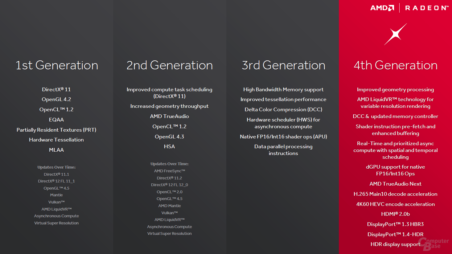
External links
- Old ATi legacy portal on the AMD domain
- AMD Radeon 6970 Performance Comparison
- Public AMD GPU specifications on X.org website
- Video Card Comparison on GPUReview.com
- TechPowerUp! GPU Database