Cache hierarchy
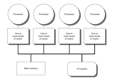
For CPU cores to run at faster clocks, we need to hide the memory latency of the main memory access. Multi-level caches are the optimum solution to provide faster access to data residing in the main memory. The access time to memory that acts as a bottleneck for the CPU core performance can be relaxed by using the hierarchical cache structure to reduce the latency and hence speed up the CPU clock.[1]
Multi-level cache
Access to the main memory for each instruction execution may result in the very slow processing with the clock speed dependent on the time taken to find the data in main memory and fetch it. In order to hide this memory latency from the processor, data caching is used. Whenever the data is required by the processor, it is fetched from the memory and stored in the small structure called Cache. For any further references to that data, the cache is searched first before going to main memory. This structure resides closer to the processor in terms of time taken to search and fetch data with respect to Main Memory. The advantages of using cache can be proven by calculating the Average Access Time (AAT) for the memory hierarchy without cache and with the cache.
Average access time (AAT)
Cache, being small in the size, may result in frequent misses and we might eventually have to go to main memory to fetch data. And hence, the AAT depends on the miss rate of all the structures that it searches through for the data.[2]

AAT for main memory is given by Hit time main memory. AAT for caches can be given by
- Hit timecache + (Miss ratecache + Miss Penaltytime taken to go to main memory after missing cache).
Hit time for caches is very less as compared to main memory and hence the resulting AAT after using cache in the memory hierarchy is improved significantly.
Trade-offs
While using the cache to improve the memory latency, it may not always result in the required improvement for the time taken to fetch data due to the way caches are organized and traversed. E.g. The same size direct mapped caches usually have more miss rate than the fully associative caches. This may also depend on upon the benchmark that we are testing the processor upon and the pattern of instructions. But always using the fully associative cache may result in more power consumption as it has to search the whole cache every time. Due to this, the trade-off between the power consumption and the size of the cache becomes critical in the cache design.[2]
Evolution
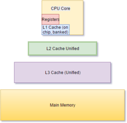
In the case of a miss in the cache, the purpose of using such a structure will be rendered useless and we will ultimately have to go to main memory to fetch the required data. The idea of using multiple levels of cache comes into picture here. This means that if we miss the cache closest to the processor, we will search for the data in the next closest level of cache and will keep on doing that until we run out of levels of caches and will finally search the main memory. The general trend is to keep L1 cache small and at a distance of 1–2 CPU clock cycles from the processor with the lower levels of caches increasing in the size to store more data than L1 and hence have lower miss rate. This, in turn, results into a better AAT. The number of levels of cache can be designed by architects as per the requirement after checking for the trade-offs between cost, AATs, and size.
Performance gains
With the technology scaling which made memory systems feasible and smaller to accommodate on a single chip, most of the modern day processors go for up to 3 or 4 levels of caches. The reduction in the AAT can be understood by this example where we check AAT for different configurations up to 3-level caches.
Example: Main memory = 50ns, L1 = 1ns (10% miss rate), L2 = 5ns (1% miss rate), L3 = 10 ns (0.2% miss rate) ·
- AAT (No cache) = 50ns
- AAT (L1 cache+ Main Memory) = 1ns + (0.1 × 50ns) = 6ns
- AAT (L1 cache + L2 cache + Main Memory) = 1ns + (0.1 × (5 + 0.01(50ns)) = 1.505ns
- AAT (L1 cache + L2 cache + L3 cache + Main Memory) = 1ns + (0.1 × (5 + 0.01(10 + 0.002 × 50ns))) = 1.5001ns
Disadvantages
- Increase in the cost of memories and hence the overall system.
- Cached data is stored only until power supply is provided.
- Increase in area consumed by memory system on chip.[3]
- In case of a large programs with poor temporal locality, even the multi-level caches cannot help improve the performance and eventually, main memory needs to be reached to fetch the data.[4]
Properties

Banked versus unified
In a banked cache, the cache is divided into instruction cache and data cache. In contrast, a unified cache contains both the instructions and data combined in the same cache. During a process, the upper-level cache is accessed to get the instructions to the processor in each cycle. The cache will also be accessed to get data. Requiring both actions to be implemented at the same time requires multiple ports in the cache and as well as takes more access time. Having multiple ports requires additional hardware and wiring leading to huge structure. Therefore, the L1 cache is organized as a banked cache which results in fewer ports, less hardware and low access time.[2]
The lower level caches L2 and L3 are accessed only when there is a miss in the L1 cache implies the frequency of access to the lower level caches is less compared to the L1 cache. Therefore, the unified organization is implemented in the lower level caches as having a single port will suffice.
Inclusion policies
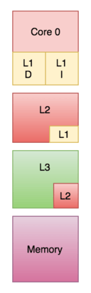
Whether a block present in the upper cache layer can be present in the lower cache level is governed by the inclusion policies below:[5]
- Inclusive
- Exclusive
- Non-Inclusive Non-Exclusive (NINE)
In the Inclusive policy, all the blocks present in the upper-level cache has to be present in the lower level cache as well. Each upper-level cache component is a subset of the lower level cache component. In this case, since there is a duplication of blocks there is some wastage of memory. However checking is better in the case of inclusive because if the lower level cache doesn't have the block then we can be sure that the upper-level cache can no way have that block.[5]
In the exclusive policy, all the cache hierarchy components are completely exclusive which implies that any element in the upper-level cache will not be present in any of the lower cache component. This enables complete usage of the cache memory as no same block is present in the other cache component. However, there is a high memory access latency.[6]
The above policies require a set on rules to be followed in order to implement them. If none of these are forced, the resulting inclusion policy is called Non-Inclusive Non-Exclusive (NINE). This means that the upper level cache may or may not be present in the lower level cache. [4]
Write policies
There are two policies which define the way in which a modified cache block will be updated in the main memory:[5]
- Write Through
- Write Back.
In the case of Write Through policy whenever the value of the cache block changes, it is further modified in the lower-level memory hierarchy as well. This policy ensures that the data is stored safely as it is written throughout the hierarchy.
However, in the case of the Write Back policy, the changed cache block will be updated in the lower-level hierarchy only when the cache block is evicted. Writing back every cache block which is evicted is not efficient. Therefore, we use the concept of a Dirty bit attached to each cache block. The dirty bit is made high whenever the cache block is modified and during eviction, only the blocks with dirty bit high will be written to the lower-level hierarchy and then the dirty bit is cleared. In this policy, there is data losing risk as the only valid copy is stored in the cache and therefore need some correction techniques to be implemented.
In case of a write where the byte is not present in the cache block the write policies below determine whether the byte has to be brought to the cache or not:[5]
- Write Allocate
- Write No-Allocate
Write Allocate policy states that in case of a write miss, the block is fetched from the main memory and placed in the cache before writing. In the Write No-Allocate policy, if the block is missed in the cache it will just write in the lower level memory hierarchy without fetching the block into the cache.
The common combinations of the policies are Write Back Write Allocate and Write Through Write No-Allocate.

Shared versus private
A private cache is private to that particular core and cannot be accessed by the other cores. Since each core has its own private cache there might be duplicate blocks in the cache which leads to reduced capacity utilization. However, this organization leads to a lower latency.[5][7][8]
A shared cache is where it is shared among multiple cores and therefore can be directly accessed by any of the cores. Since it is shared, each block in the cache is unique and therefore has more hit rate as there will be no duplicate blocks. However, the cache hit latency is larger as multiple cores try to access the same cache.
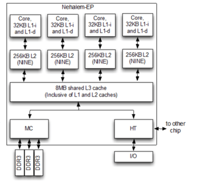
In the multi-core processors, the organization of the cache to be shared or private impacts the performance of the processor. In practice, the upper-level cache L1 (or sometimes L2)[9][10] is implemented as private and lower level caches are implemented as shared.
Recent implementation models
Intel Broadwell Microarchitechture (2014)
- L1 Cache (Instruction and Data) – 64kB per core
- L2 Cache – 256kB per core
- L3 Cache – 2MB to 6MB shared
- L4 Cache – 128MB of eDRAM (Iris Pro Models only)[9]
Intel Kaby Lake Microarchitechture (2016)
- L1 Cache (Instruction and Data) – 64kB per core
- L2 Cache – 256kB per core
- L3 Cache – 8192kB shared[10]
IBM Power 7
- L1 Cache (Instruction and Data) – Each 64-banked, each bank has 2rd+1wr ports 32kB, 8-way associative, 128B block, Write through
- L2 Cache – 256kB, 8-way, 128B block, Write back, Inclusive of L1, 2ns access latency
- L3 Cache – 8 regions of 4MB (total 32MB), local region 6ns, remote 30ns, each region 8-way associative, DRAM data array, SRAM tag array[12]
See also
- Power7
- Intel Broadwell Microarchitecture
- Intel Kaby Lake Microarchitecture
- CPU Cache
- Memory hierarchy
- CAS latency
- Cache (computing)
References
- ↑ "Cache: Why Level It" (PDF).
- 1 2 3 Hennessey and Patterson. Computer Architecture: A Quantitative Approach. Morgan Kauffman. ISBN 9780123704900.
- ↑ "Memory Hierarchy".
- 1 2 Solihin, Yan (2016). Fundamentals of Parallel Multicore Architecture. Chapman and Hall. pp. Chapter 5: Introduction to Memory Hierarchy Organization. ISBN 9781482211184.
- 1 2 3 4 5 Solihin, Yan (2009). Fundamentals of Parallel Computer Architecture. Solihin Publishing. pp. Chapter 6: Introduction to Memory Hierarchy Organization. ISBN 9780984163007.
- ↑ "Performance Evaluation of Exclusive Cache Hierarchies" (PDF).
- ↑ "Software Techniques for Shared-Cache Multi-Core Systems".
- ↑ "An Adaptive Shared/Private NUCA Cache Partitioning Scheme for Chip Multiprocessors" (PDF).
- 1 2 "Intel Broadwell Microarchitecture".
- 1 2 "Intel Kaby Lake Microrchitecture".
- ↑ "The Architecture of the Nehalem Processor and Nehalem-EP SMP Platforms" (PDF).
- ↑ "IBM Power7".