Avalanche transistor
An avalanche transistor is a bipolar junction transistor designed for operation in the region of its collector-current/collector-to-emitter voltage characteristics beyond the collector-to-emitter breakdown voltage, called avalanche breakdown region. This region is characterized by avalanche breakdown, a phenomenon similar to Townsend discharge for gases, and negative differential resistance. Operation in the avalanche breakdown region is called avalanche-mode operation: it gives avalanche transistors the ability to switch very high currents with less than a nanosecond rise and fall times (transition times). Transistors not specifically designed for the purpose can have reasonably consistent avalanche properties; for example 82% of samples of the 15V high-speed switch 2N2369, manufactured over a 12-year period, were capable of generating avalanche breakdown pulses with rise time of 350 ps or less, using a 90V power supply as Jim Williams writes.[1][2]
History
The first paper dealing with avalanche transistors was Ebers & Miller (1955): the paper describes how to use alloy-junction transistors in the avalanche breakdown region, in order to overcome speed and breakdown voltage limitations which affected the first models of such kind of transistor when used in earlier computer digital circuits. Therefore the very first applications of avalanche transistors were in switching circuits and multivibrators. The introduction of the avalanche transistor served also as an application of Miller's empirical formula for the avalanche multiplication coefficient , first introduced in the paper Miller (1955): the need of better understanding transistor behavior in the avalanche breakdown region, not only for using them in avalanche mode, gave rise to an extensive research on impact ionization in semiconductors (see Kennedy & O'Brien (1966)). From the beginning of the 1960s to the first half of the 1970s, several avalanche-transistor circuits were proposed, and also it was studied what kind of bipolar junction transistor is best suited for the use in the avalanche breakdown region: a complete reference, which includes also the contributions of scientists from ex-USSR and COMECON countries, is the book by Дьяконов (Dyakonov) (1973). The first application of the avalanche transistor as a linear amplifier, named Controlled Avalanche Transit Time Triode, (CATT) was described in (Eshbach, Se Puan & Tantraporn 1976): a similar device, named IMPISTOR was described more or less in the same period in the paper of Carrol & Winstanley (1974). Linear applications of this class of devices started later since there are some requirements to fulfill, as described below: also, the use of avalanche transistor in those applications is not mainstream since the devices require high collector to emitter voltages in order to work properly. Nowadays, there is still active research on avalanche devices (transistors or other) made of compound semiconductors, being capable of switching currents of several tens of amperes even faster than "traditional" avalanche transistors.

Basic theory
Static avalanche region characteristics
In this section, the static characteristic of an avalanche transistor is calculated. For the sake of simplicity, only an NPN device is considered: however, the same results are valid for PNP devices only changing signs to voltages and currents accordingly. The analysis closely follows that of William D. Roehr in (Roehr 1963). Since avalanche breakdown multiplication is present only across the collector-base junction, the first step of the calculation is to determine collector current as a sum of various component currents though the collector since only those fluxes of charge are subject to this phenomenon. Kirchhoff's current law applied to a bipolar junction transistor implies the following relation, always satisfied by the collector current


while for the same device working in the active region, basic transistor theory gives the following relation

where
- is the base current,
- is the collector-base reverse leakage current,
- is the emitter current,
- is the common emitter current gain of the transistor.


Equating the two formulas for gives the following result

and since is the common base current gain of the transistor, then


When avalanche effects in a transistor collector are considered, the collector current is given by

where is Miller's avalanche multiplication coefficient. It is the most important parameter in avalanche mode operation: its expression is the following

where
- is the collector-base breakdown voltage,
- is a constant depending on the semiconductor used for the construction of the transistor and doping profile of the collector-base junction,
- is the collector-base voltage.


Using again Kirchhoff's current law for the bipolar junction transistor and the given expression for , the resulting expression for is the following

and remembering that and where is the base-emitter voltage


since : this is the expression of the parametric family of the collector characteristics with parameter . Note that increases without limit if

![\left({\frac {V_{{CE}}}{BV_{{CBO}}}}\right)^{{\!n}}=1-\alpha \iff V_{{CE}}=BV_{{CEO}}={\sqrt[ {n}]{(1-\alpha )}}BV_{{CBO}}={\frac {BV_{{CBO}}}{{\sqrt[ {n}]{\beta +1}}}}](../I/m/2934adf1e151798d2ed6372c3a0c694d1f977a20.svg)
where is the collector-emitter breakdown voltage. Also, it is possible to express as a function of , and obtain an analytical formula for the collector-emitter differential resistance by straightforward differentiation: however, the details are not given here.


Differential dynamical model
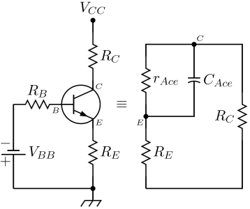
The differential dynamical mode described here, also called the small signal model, is the only intrinsic small signal model of the avalanche transistor. Stray elements due to the package enclosing the transistor are deliberately neglected, since their analysis would not add anything useful from the point of view of the working principles of the avalanche transistor. However, when realizing an electronic circuit, those parameters are of great importance. Particularly, stray inductances in series with collector and emitter leads have to be minimized to preserve the high speed performance of avalanche transistor circuits. Also, this equivalent circuit is useful when describing the behavior of the avalanche transistor near its turn on time, where collector currents and voltages are still near their quiescent values: in the real circuit it permits the calculation of time constants and therefore rise and fall times of the waveform. However, since avalanche transistor switching circuits are intrinsically large signal circuits, the only way to predict with reasonable accuracy their real behaviour is to do numerical simulations. Again, the analysis closely follows that of William D. Roehr in (Roehr 1963).
An avalanche transistor operated by a common bias network is shown in the picture on the right: can be zero or positive value, while can be short circuited. In every avalanche transistor circuit, the output signal is taken from the collector or the emitter: therefore the small-signal differential model of an avalanche transistor working in the avalanche region is always seen from the collector-emitter output pins, and consist of a parallel circuit as shown in the picture on the right, which includes only bias components. The magnitude and sign of both those parameters are controlled by the base current : since both base-collector and base-emitter junctions are inversely biased in the quiescent state, the equivalent circuit of the base input is simply a current generator shunted by base-emitter and base-collector junction capacitances and is therefore not analyzed in what follows. The intrinsic time constant of the basic equivalent small signal circuit has the following value


where
- is the collector-emitter avalanche differential resistance and, as stated above, can be obtained by differentiation of the collector-emitter voltage respect to the collector current , for a constant base current


- is the collector-emitter avalanche differential capacitance and has the following expression

- where
- is the current gain angular cutoff frequency
- is the common base output capacitance


The two parameters are both negative. This means that if the collector load const of an ideal current source, the circuit is unstable. This is the theoretical justification of the astable multivibrator behavior of the circuit when the voltage is raised over some critical level.

Second breakdown avalanche mode
When the collector current rises above the data sheet limit a new breakdown mechanism become important: the second breakdown. This phenomenon is caused by excessive heating of some points (hot spots) in the base-emitter region of the bipolar junction transistor, which give rise to an exponentially increasing current through these points: this exponential rise of current in turn gives rise to even more overheating, originating a positive thermal feedback mechanism. While analyzing the static characteristic, the presence of this phenomenon is seen as a sharp collector voltage drop and a corresponding almost vertical rise of the collector current. At the present, it is not possible to produce a transistor without hot spots and thus without second breakdown, since their presence is related to the technology of refinement of silicon. During this process, very small but finite quantities of metals remain in localized portions of the wafer: these particles of metals became deep centers of recombination, i.e. centers where current exists in a preferred way. While this phenomenon is destructive for Bipolar junction transistors working in the usual way, it can be used to push-up further the current and voltage limits of a device working in avalanche mode by limiting its time duration: also, the switching speed of the device is not negatively affected. A clear description of avalanche transistor circuits working in second breakdown regime together with some examples can be found in the paper Baker (1991).

Numerical simulations
Avalanche transistor circuits are intrinsically large signal circuits, so small signal models, when applied to such circuits, can only give a qualitative description. To obtain more accurate information about the behavior of time dependent voltages and currents in such circuits it is necessary to use numerical analysis. The "classical" approach, detailed in the paper Дьяконов (Dyakonov) (2004b) which relies upon the book Дьяконов (Dyakonov) (1973), consists in considering the circuits as a system of nonlinear ordinary differential equations and solve it by a numerical method implemented by a general purpose numerical simulation software: results obtained in this way are fairly accurate and simple to obtain. However, this methods rely on the use of analytical transistor models best suited for the analysis of the breakdown region: those models are not necessarily suited to describe the device working in all possible regions. A more modern approach is to use the common analog circuit simulator SPICE together with an advanced transistor model supporting avalanche breakdown simulations, which the basic SPICE transistor model does not. Examples of such models are described in the paper Keshavarz, Raney & Campbell (1993) and in the paper Kloosterman & De Graaff (1989): the latter is a description of the Mextram model, currently used by some semiconductor industries to characterize their bipolar junction transistors.
A graphical method
A graphical method for studying the behavior of an avalanche transistor was proposed in references Spirito (1968) and Spirito (1971): the method was first derived in order to plot the static behavior of the device and then was applied also to solve problems concerning the dynamic behavior. The method bears the spirit of the graphical methods used to design tube and transistor circuits directly from the characteristic diagrams given in data sheets by producers.
Applications
Avalanche transistors are mainly used as fast pulse generators, having rise and fall times of less than a nanosecond and high output voltage and current. They are occasionally used as amplifiers in the microwave frequency range, even if this use is not mainstream: when used for this purpose, they are called "Controlled Avalanche Transit-time Triodes" (CATTs).
Avalanche mode switching circuits
Avalanche mode switching relies on avalanche multiplication of current flowing through the collector-base junction as a result of impact ionization of the atoms in the semiconductor crystal lattice. Avalanche breakdown in semiconductors has found application in switching circuits for two basic reasons
- it can provide very high switching speeds, since current builds-up in very small times, in the picosecond range, due to avalanche multiplication.
- It can provide very high output currents, since large currents can be controlled by very small ones, again due to avalanche multiplication.
The two circuits considered in this section are the simplest examples of avalanche transistor circuits for switching purposes: both the examples detailed are monostable multivibrators. There are several more complex circuits in the literature, for example in the books Roehr (1963) and Дьяконов (Dyakonov) (1973).
Most circuits employing an avalanche transistor are activated by the following two different kinds of input:


- Collector triggering input circuit: the input trigger signal is fed to the collector via a fast switching diode , possibly after being shaped by a pulse shaping network. This way of driving an avalanche transistor was extensively employed in first generation circuits since the collector node has a high impedance and also collector capacitance behaves quite linearly under large signal regime. As a consequence of this, the delay time from input to output is very small and approximately independent of the value of control voltage. However, this trigger circuit requires a diode capable of resist to high reverse voltages and switch very fast, characteristics that are very difficult to realize in the same diode, therefore it is rarely seen in modern avalanche transistor circuits.
- Base triggering input circuit: the input trigger signal is fed directly to the base via a fast switching diode , possibly after being shaped by a pulse shaping network. This way of driving an avalanche transistor was relatively less employed in first generation circuits because the base node has a relatively low impedance and an input capacitance which is highly nonlinear (as a matter of fact, it is exponential) under the large signal regime: this causes a fairly large, input voltage dependent, delay time, which was analyzed in detail in the paper Spirito (1974). However, the required inverse voltage for the feed diode is far lower respect diodes to be used in collectior trigger input circuits, and since ultra fast Schottky diodes are easily and cheaply found, this is the driver circuit employed in most modern avalanche transistor circuit. This is also the reason why the diode in the following applicative circuits is symbolized as a Schottky diode.


Avalanche transistor can also be triggered by lowering the emitter voltage , but this configuration is rarely seen in the literature and in practical circuits.: in reference Meiling & Stary (1968), paragraph 3.2.4 "Trigger circuits" one such configuration is described, where the avalanche transistor is used itself as a part of the trigger circuit of a complex pulser, while in reference Дьяконов (Dyakonov) (1973, pp. 185) a balanced level discriminator where a common bipolar junction transistor is emitter-coupled to an avalanche transistor is briefly described.

The two avalanche pulser described below are both base triggered and have two outputs. Since the device used is an NPN transistor, is a positive going output while is a negative going output: using a PNP transistor reverses the polarities of outputs. The description of their simplified versions, where resistor or is set to zero ohm (obviously not both) in order to have a single output, can be found in reference Millman & Taub (1965). Resistor recharges the capacitor or the transmission line (i.e. the energy storage components) after commutation. It has usually a high resistance to limit the static collector current, so the recharging process is slow. Sometimes this resistor is replaced by an electronic circuit which is capable of charging faster the energy storage components. However this kind of circuit usually is patented so they are rarely found in mainstream application circuits.


- Capacitor discharge avalanche pulser: a trigger signal applied to the base lead of the avalanche transistor cause the avalanche breakdown between the collector and emitter lead. The capacitor starts to be discharged by a current flowing through the resistors and : the voltages across those resistors are the output voltages. The current waveform is not a simple RC discharge current but has a complex behavior which depends on the avalanche mechanism: however it has a very fast rise time, of the order of fractions of a nanosecond. Peak current depends on the size of the capacitor : when its value is raised over a few hundred picofarads, transistor goes in to second breakdown avalanche mode, and peak currents reach values of several amperes.
- Transmission line avalanche pulser: a trigger signal applied to the base lead of the avalanche transistor cause the avalanche breakdown between the collector and emitter lead. The fast rise time of the collector current generates a current pulse of approximatively the same amplitude, which propagates along the transmission line. The pulse reaches the open circuited end of the line after the characteristic delay time of the line has elapsed, and then is reflected backward. If the characteristic impedance of the transmission line is equal to the resistances and , the backward reflected pulse reaches the beginning of the line and stops. As a consequence of this traveling wave behavior, the current flowing through the avalanche transistor has a rectangular shape of duration


In practical designs, an adjustable impedance like a two terminal Zobel network (or simply a trimmer capacitor) is placed from the collector of the avalanche transistor to ground, giving the transmission line pulser the ability to reduce ringing and other undesidered behavior on the output voltages.

It is possible to turn those circuits into astable multivibrators by removing their trigger input circuits and
- raising their power supply voltage until a relaxation oscillation begins, or
- connecting the base resistor to a positive base bias voltage and thus forcibly starting avalanche breakdown and associated relaxation oscillation.

A well-detailed example of the first procedure is described in reference Holme (2006). It is also possible to realize avalanche mode bistable multivibrators, but their use is not as common as other types described of multivibrators, one important reason being that they require two avalanche transistors, one working continuously in avalanche breakdown regime, and this can give serious problems from the point of wiev of power dissipation and device operating life.
A practical, easily realised, and inexpensive application is the generation of fast-rising pulses for checking equipment rise time.[1][3]
The controlled avalanche transit-time triode (CATT)
Avalanche mode amplification relies on avalanche multiplication as avalanche mode switching. However, for this mode of operation, it is necessary that Miller's avalanche multiplication coefficient be kept almost constant for large output voltage swings: if this condition is not fulfilled, significant amplitude distortion arises on the output signal. Consequently
- avalanche transistors used for application in switching circuits cannot be used since Miller's coefficient varies widely with the collector to emitter voltage
- the operating point of the device cannot be in the negative resistance of the avalanche breakdown region for the same reason
These two requirements imply that a device used for amplification need a physical structure different from that of a typical avalanche transistor. The Controlled Avalanche Transit-time Triode (CATT), designed for microwave amplification, has a quite large lightly-doped region between the base and the collector regions, giving the device a collector-emitter breakdown voltage fairly high compared to bipolar transistors of the same geometry. The current amplification mechanism is the same of the avalanche transistor, i.e. carrier generation by impact ionization, but there is also a transit-time effect as in IMPATT and TRAPATT diodes, where a high-field region travels along the avalanching junction, precisely in along the intrinsic region. The device structure and choice of bias point imply that
- Miller's avalanche multiplication coefficient M is limited to about 10.
- The transit-time effect keeps this coefficient almost constant and independent of the collector-to-emitter voltage.
The theory for this kind of avalanche transistor is described completely in the paper Eshbach, Se Puan & Tantraporn (1976), which also shows that this semiconductor device structure is well suited for microwave power amplification. It can deliver several watts of radio frequency power at a frequency of several gigahertz and it also has a control terminal, the base. However, it is not widely used since it requires voltages exceeding 200 volts to work properly, while gallium arsenide or other compound semiconductor FETs deliver a similar performance while being easier to work with. A similar device structure, proposed more or less in the same period in the paper Carrol & Winstanley (1974), was the IMPISTOR, being a transistor with IMPATT collector-base junction.

See also
Notes
- 1 2 "Linear Technology AN47" Archived March 20, 2012, at the Wayback Machine., High-speed amplifier techniques, 1991, Appendix D: Measuring probe-oscilloscope response.
- ↑ "Linear Technology AN94", Slew Rate Verification for Wideband Amplifiers The Taming of the Slew"
- ↑ iceNINE Tech: Homebrew Really Fast Pulse Generator
References
- Baker, R. Jacob (1991), "High voltage pulse generation using current mode second breakdown in a bipolar junction transistor", Review of Scientific Instruments, The American Institute of Physics, 62: 1031–1036, doi:10.1063/1.1142054. A clear description of avalanche transistor circuits working in the second breakdown region (restricted access): however, a copy from the author's website is available here.
- Eshbach, John R.; Se Puan, Yu; Tantraporn, Wirojana (1976), "Theory of a new three-terminal microwave power amplifier", IEEE Transactions on Electron Devices, IEEE, 23: 332–343, doi:10.1109/t-ed.1976.18401. The first article describing the working principles and potential applications of the CATT (restricted access).
- Meiling, Wolfgang; Stary, Franz (1968), Nanosecond pulse techniques, New York-London-Paris: Gordon & Breach Science Publishers. Sections 3.1.5 "Avalanche transistors", 3.2 and 3.4 "Trigger circuits containing avalanche transistors".
- Millman, Jacob; Taub, Herbert (1965), Pulse, digital and switching waveforms, New York-St. Louis-San Francisco-Toronto-London-Sydney: McGraw-Hill Book Company External link in
|publisher=(help). Mainly sections 6.9, 6.10, 12.10, 13,16, 13.17. - Roehr, William D. (1963), High-speed switching transistor handbook (3rd printing ed.), Phoenix: Motorola, Inc.. Chapter 9 "Avalanche mode switching".
- The ZTX413 Avalanche Transistor Zetex Semiconductor Design Note 24, October 1995.
- The ZTX413 Avalanche Transistor Zetex Semiconductor Data Sheet, March 1994.
- The ZTX415 Avalanche Mode Transistor Zetex Semiconductors Application Note 8, January 1996.
Bibliography
- Ebers, J. J.; Miller, S. L. (1955), "Alloyed Junction Avalanche Transistors" (PDF), Bell System Technical Journal, 34 (5): 883–902, doi:10.1002/j.1538-7305.1955.tb03783.x. The first paper analyzing the use of bipolar junction transistors in the avalanche region.
- Kennedy, D. P.; O'Brien, R. R. (1966), "Avalanche Breakdown Calculations for a Planar p-n Junction", IBM Journal of Research and Development, 10: 213–219, doi:10.1147/rd.103.0213. A paper containing an accurate analysis of the avalanche breakdown phenomenon in planar pn-junctions, as those found in almost all modern transistors.
- Miller, S. L. (1955), "Avalanche Breakdown in Germanium", Physical Review, 99: 1234–1241, doi:10.1103/physrev.99.1234. The paper where the above formula for the avalanche multiplication coefficient M first appeared (restricted access).
- Dyakonov, Vladimir Pavlovich (1973), Лавинные транзисторы и их применение в импульсных устройствах, Советское радио (Sovetskoe Radio) (Zipped djvu format). "Avalanche transistors and their application in pulse circuits" is a very scarce book worth a look, especially for the Russian reader: in-dept coverage of the theory of avalanche transistor, analysis of practical circuits, and a rich bibliography of 125 titles.
- Dyakonov, Vladimir Pavlovich (2008), Лавинные транзисторы и тиристоры. теория и применение, Москва.СОЛОН-Пресс (Moscow. SOLON-Press), archived from the original on 2008-05-01. "Avalanche transistors and tyristors. Theory and applications": a recent book on the same subject.
External links
Theory
- Carrol, J. E.; Winstanley, H. C. (1974), "Transistor improvements using an IMPATT collector", Electronics Letters, IEEE, 10: 516–518. A paper proposing and describing the IMPISTOR, a semiconductor device similar to the CATT.
- Дьяконов (Dyakonov), Владимир Павлович (Vladimir Pavlovich) (2004a), "Анализ статических вольтамперных характеристик диодов и транзисторов с учетом лавинного пробоя (Analysis of static volt-amperometric characteristics of diodes and transistors including avalanche breakdown)", Exponenta.ru. A paper analyzing the volt-amperometric characteristic of diodes and transistors using the computer algebra program Mathematica.
- Дьяконов (Dyakonov), Владимир Павлович (Vladimir Pavlovich) (2004b), "Расчет параметров импульсов емкостного релаксатора на лавинном транзисторе (Calculation of pulse parameters as a function of capacity in an avalanche transistor relaxation oscillator)", Exponenta.ru. A paper about the design of an avalanche transistor relaxation oscillator using the computer algebra program Mathematica
- Hamilton, Douglas J.; Gibbons, James F.; Shockley, Walter (1959), "Physical principles of avalanche transistor pulse circuits", IRE Solid-State Circuits Conference, Volume II, pp. 92–93, doi:10.1109/ISSCC.1959.1157029. A brief description of the basic physical principles of avalanche transistor circuits: instructive and interesting but "restricted access".
- Huang, Jack S. T. (1967), "Study of Transistor Switching Circuit Stability in the Avalanche Region", IEEE Journal of Solid State Circuits, 2 (1): 10–21, doi:10.1109/jssc.1967.1049775. A theoretical study of the stability of a transistor biased in the avalanche region (restricted access).
- Keshavarz, A.A.; Raney, C.W.; Campbell, D.C. (August 1, 1993), Report SAND--93-0241C. A breakdown model for the bipolar transistor to be used with circuit simulators (PDF), Sandia National Laboratories available from the U.S. Department of Energy Office of Scientific & Technical Information. A report describing a transistor model capable of including avalanche effects in SPICE simulations.
- Kloosterman, W. J.; De Graaff, H. C. (1989), "Avalanche multiplication in a compact bipolar transistor model for circuit simulation", IEEE Transactions on Electron Devices, IEEE, 36 (7): 1376–1380, doi:10.1109/16.30944. A paper describing the Mextram SPICE model from the point of view of avalanche behavior simulation. For a free copy found in the Mextram home page of NXP see here.
- Rickelt, M.; Rein, H. M. (2002), "A novel transistor model for simulating avalanche-breakdown effects in Si bipolar circuits", IEEE Journal of Solid State Circuits, IEEE, 37 (9): 1184–1197. A paper describing a transistor model for bipolar circuit simulation including avalanche effects (restricted access).
- Jochen Riks "Avalanche-Transistor" (in German). A brief description of the working principles of the avalanche transistor, part of the course "Impulsschaltungen F-Praktikum EXP 10", June 1996, Fachschaft Physik Uni Düsseldorf.
- Spirito, Paolo (1968), "Direct Current-Voltage Characteristics of Transistors in the Avalanche Region", IEEE Journal of Solid State Circuits, 3 (2): 194–195, doi:10.1109/jssc.1968.1049869. A paper proposing a graphical method to plot the static characteristic of an avalanche transistor (restricted access).
- Spirito, Paolo (1971), "Static and dynamic behaviour of transistors in the avalanche region", IEEE Journal of Solid State Circuits, 6 (2): 83–87, doi:10.1109/jssc.1971.1049655. A paper pushing further the study of avalanche transistor by a graphical method proposed in the preceding work (restricted access).
- Spirito, Paolo (1974), "On the trigger delay of avalanche transistors", IEEE Journal of Solid State Circuits, 9 (5): 307–309, doi:10.1109/jssc.1974.1050518. A paper analyzing the trigger delay time of avalanche transistors by means of numerical analysis (restricted access).
- Spirito, Paolo; Vitale, G. F. (1972), "An analysis of the dynamic behavior of switching circuits using avalanche transistors", IEEE Journal of Solid State Circuits, 7 (4): 315–320, doi:10.1109/jssc.1972.1050310. A paper where an analytical model of the behavior of an avalanche transistor is derived after suitable approximations (restricted access).
Applications
- Biddle, Wade; Lonobile, David (1997), "Sweep Deflection Circuit Development Using Computer-Aided Circuit Design for the OMEGA Multichannel Streak Camera" (PDF), LLE Review, 73: 6–14. A paper describing a fast sweep generator for a streak camera constructed using series connected avalanche transistor circuits.
- Chaplin, G. B. B. (1958), "A method of designing transistor avalanche circuits with application to a sensitive transistor oscilloscope", IRE Solid-State Circuits Conference, Volume I, pp. 21–23, doi:10.1109/ISSCC.1958.1155606. A paper describing an application of avalanche transistors to the design of a sampling oscilloscope: available abstract, full paper is "restricted access".
- Fulkerson, E. Stephen; Norman, Douglas C.; Booth, Rex (May 28, 1997), Report UCRL-JC--125874 - Driving Pockels cells using avalanche transistors, Lawrence Livermore National Laboratory. Available from the U.S. Department of Energy Office of Scientific & Technical Information. A report describing the design of a driver for Pockels cells Q-switches.
- Holme, Andrew (2006), Avalanche transistor pulse generator, retrieved 23 April 2008. A project, inspired to Jim Williams' Linear Technology application notes AN72 and AN94, of an avalanche transistor astable multivibrator with schematics, waveforms and photos of the layout.
- Kilpelä, Ari (2004), Pulsed time-of-flight laser range finder techniques for fast, high precision measurement applications, Acta Universitatis Ouluensis Technica, 197, Oolu: University of Oulu, ISBN 951-42-7261-7. Academic Dissertation presented with the assent of the Faculty of Technology. A doctoral dissertation describing a Laser TOF (Time Of Flight) Radar and its construction using an avalanche transistor pulser.
- Kilpelä, Ari; Kostamovaara, Juha (1997), "Laser pulser for a time-of-flight laser radar", Review of Scientific Instruments, The American Institute of Physics, 68 (6): 2253–2258 (preprint version here). A paper describing an avalanche transistor pulser and its use as Laser driver in a laser radar.
- NXP Mextram home page A very rich repository of documents about the Mextram bipolar junction transistor SPICE model, capable of avalanche breakdown behavior simulation.
- "Operating the pulsed laser diode SPL LLxx", "Range finding using pulsed laser diodes" OSRAM Opto Semiconductors GmbH Application Notes, 2004-09-10. Two application notes from Osram Opto Semiconductors describing pulsed operation of a Laser diode, using avalanche transistors and other kind of drivers.
- Pellegrin, J. L. (September 1969), SLAC-PUB-0669 - Increasing the Stability of Series Avalanche Transistor Circuits, Stanford Linear Accelerator Center, archived from the original on 2004-12-26. A paper describing a method to enhance performances of banks of series-connected avalanche transistor circuits.
- Williams, Jim (2003), "The taming of the slew", EDN Magazine (25 September): 57–65, archived from the original on 2006-06-28 (for a PDF copy, see here). A detailed paper describing the construction and performance of an avalanche transistor pre-trigger pulse generator to test the slew-rate of very fast operational amplifiers. Also appeared under the title "Slew Rate Verification for Wideband Amplifiers - The Taming of the Slew", application note AN94, Linear Technology, May 2003. See also, from the same author, Linear Technology application note AN47, High speed amplifier techniques", August 1991, where an astable circuit similar to that described by Holme is detailed in appendix D, pages 93–95.
Varia
- R. Jacob Baker Academic Web Page at University of Nevada, Las Vegas. A contributor to the theory and applications of avalanche transistors.
- Владимир Павлович Дьяконов (Vladimir Pavlovich D'yakonov) (in Russian). Some biographical notes about one of the leading contributors to the theory and application of avalanche transistors.
- Ari Kilpelä Academic Web Page at the University of Oulu. A researcher working on theory and applications of avalanche transistor circuits.