Intel 8088
|
An Intel 8088 microprocessor | |
| Produced | From 1979 to 1990s |
|---|---|
| Max. CPU clock rate | 5 MHz to 10 MHz |
| Min. feature size | 3 μm |
| Instruction set | 8086 (16-bit x86) |
| Model | 8088 Series |
| Predecessor |
Intel 8080 Intel 8085 |
| Successor |
Intel 80188 Intel 80186 |
| Package(s) | |
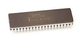
The Intel 8088 ("eighty-eighty-eight", also called iAPX 88)[1][2][3] microprocessor is a variant of the Intel 8086. Introduced on July 1, 1979, the 8088 had an 8-bit external data bus instead of the 16-bit bus of the 8086. The 16-bit registers and the one megabyte address range were unchanged, however. In fact, according to the Intel documentation, the 8086 and 8088 have the same execution unit (EU)—only the bus interface unit (BIU) is different. The original IBM PC was based on the 8088.
History and description
The 8088 was designed in Israel, at Intel's Haifa laboratory, as with a large number of Intel's processors.[4] The 8088 was targeted at economical systems by allowing the use of an 8-bit data path and 8-bit support and peripheral chips; complex circuit boards were still fairly cumbersome and expensive when it was released. The prefetch queue of the 8088 was shortened to four bytes, from the 8086's six bytes, and the prefetch algorithm was slightly modified to adapt to the narrower bus.[lower-alpha 1] These modifications of the basic 8086 design were one of the first jobs assigned to Intel's then new design office and laboratory in Haifa, Israel.
Variants of the 8088 with more than 5 MHz maximum clock frequency include the 8088-2, which was fabricated using Intel's new enhanced nMOS process called HMOS and specified for a maximum frequency of 8 MHz. Later followed the 80C88, a fully static CHMOS design, which could operate with clock speeds from 0 to 8 MHz. There were also several other, more or less similar, variants from other manufacturers. For instance, the NEC V20 was a pin compatible and slightly faster (at the same clock frequency) variant of the 8088, designed and manufactured by NEC. Successive NEC 8088 compatible processors would run at up to 16 MHz. In 1984, Commodore International signed a deal to manufacture the 8088 for use in a licensed Dynalogic Hyperion clone, in a move that was regarded as signalling a major new direction for the company.[5]
When announced, the list price of the 8088 was US $124.80.[6]
Differences from the 8086
The 8088 is architecturally very similar to the 8086. The main difference is that there are only 8 data lines instead of the 8086's 16 lines. All of the other pins of the device perform the same function as they do with the 8086 with two exceptions. First, pin 34 is no longer BHE (this is the high order byte select on the 8086—the 8088 does not have a high order byte on its 8 bit data bus).[7]:5–97 Instead it outputs a maximum mode status, SSO. Combined with the IO/M and DT/R signals, the bus cycles can be decoded (It generally indicates when a write operation or an interrupt is in progress). The second change is the pin that signals if a memory access or input/output access is being made has had it sense reversed. The pin on the 8088 is IO/M. On the 8086 part it is IO/M. The reason for the reversal is that it makes the 8088 compatible with the 8085.[7]:5–98
Performance
Depending on the clock frequency, the number of memory wait states, as well as on the characteristics of the particular application program, the average performance for the Intel 8088 ranged from approximately 0.33–1 million instructions per second.[8] Meanwhile, the mov reg,reg and ALU[lower-alpha 2] reg,reg instructions taking two and three cycles respectively yielded an absolute peak performance of between 1/3 and 1/2 MIPS per MHz, that is, somewhere in the range 3–5 MIPS at 10 MHz.
The speed of the execution unit (EU) and the bus of the 8086 CPU was well balanced; with a typical instruction mix, an 8086 could execute instructions out of the prefetch queue a good bit of the time. Cutting down the bus to 8 bits made it a serious bottleneck in the 8088. With the speed of instruction fetch reduced by 50% in the 8088 as compared to the 8086, a sequence of fast instructions can quickly drain the 4-byte prefetch queue. When the queue is empty, instructions take as long to complete as they take to fetch. Both the 8086 and 8088 take four clock cycles to complete a bus cycle; whereas for the 8086 this means 4 clocks to transfer 2 bytes, on the 8088 it is 4 clocks per byte. Therefore, for example, a 2-byte shift or rotate instruction, which takes the EU only 2 clock cycles to execute, actually takes eight clocks to complete if it is not in the prefetch queue. A sequence of such fast instructions prevents the queue from being filled as fast as it is drained, and In general, because so many basic instructions execute in fewer than four clocks per instruction byte—including almost all the ALU and data-movement instructions on register operands and some of these on memory operands—it is practically impossible to avoid idling the EU in the 8088 at least 1/4 of the time while executing useful real-world programs, and it is not hard to idle it half the time. In short, an 8088 typically runs about half as fast as 8086 clocked at the same rate, because of the bus bottleneck (the only major difference).
A side effect of the 8088 design, with the slow bus and the small prefetch queue, is that the speed of code execution can be very dependent on instruction order. When programming the 8088, for CPU efficiency, it is vital to interleave long-running instructions with short ones whenever possible. For example, a repeated string operation or a shift by three or more will take long enough to allow time for the 4-byte prefetch queue to completely fill. If short instructions (i.e. ones totaling few bytes) are placed between slower instructions like these, the short ones can execute at full speed out of the queue. If, on the other hand, the slow instructions are executed sequentially, back to back, then after the first of them the bus unit will be forced to idle because the queue will already be full, with the consequence that later more of the faster instructions will suffer fetch delays that might have been avoidable. As some instructions, such as single-bit-position shifts and rotates, take literally 4 times as long to fetch as to execute,[lower-alpha 3] the overall effect can be a slowdown by a factor of two or more. If those code segments are the bodies of loops, the difference in execution time may be very noticeable on the human timescale.
The 8088 is also (like the 8086) slow at accessing memory. The same ALU that is used to execute arithmetic and logic instructions is also used to calculate effective addresses. (There is a separate adder for adding a shifted segment register to the offset address, but the offset EA itself is always calculated entirely in the main ALU.) Furthermore, the loose coupling of the EU and BIU (bus unit) inserts communication overhead between the units, and the four clock period bus transfer cycle is not particularly streamlined. (Contrast the two clock period bus cycle of the 6502 CPU and the 80286's three clock period bus cycle with pipelining down to two cycles for most transfers.) Most 8088 instructions that can operate on either registers or memory, including common ALU and data-movement operations, are at least four times slower for memory operands than for only register operands. Therefore, efficient 8088 (and 8086) programs avoid repeated access of memory operands when possible, loading operands from memory into registers to work with them there and storing back only the finished results. The relatively large general register set of the 8088 compared to its contemporaries assists this strategy. When there are not enough registers for all variables that are needed at once, saving registers by pushing them onto the stack and popping them back to restore them is the fastest way to use memory to augment the registers, as the stack PUSH and POP instructions are the fastest memory operations. (The same is probably not true on the 80286 and later; they have dedicated address ALUs and perform memory accesses much faster than the 8088 and 8086.)
Finally, because calls, jumps, and interrupts reset the prefetch queue, and because loading the IP register requires communication between the EU and the BIU (since the IP register is in the BIU, not in the EU where the general registers are), these operations are costly. All jumps and calls take at least 15 clock cycles. Any conditional jump requires 4 clock cycles if not taken, but if taken it requires 16 cycles in addition to resetting the prefetch queue; therefore, conditional jumps should be arranged to be not taken most of the time, especially inside loops. In some cases, a sequence of logic and movement operations is faster than a conditional jump that skips over one or two instructions to achieve the same result.
Intel datasheets for the 8086 and 8088 advertised the dedicated multiply and divide instructions (MUL, IMUL, DIV, and IDIV), but they are very slow, on the order of 100-200 clock cycles each. Many simple multiplications by small constants (besides powers of two, for which shifts can be used) can be done much faster using dedicated short subroutines. (The 80286 and 80386 each greatly increased the execution speed of these multiply and divide instructions.)[lower-alpha 4]
Selection for use in the IBM PC
The original IBM PC was the most influential microcomputer to use the 8088. It used a clock frequency of 4.77 MHz (4/3 the NTSC colorburst frequency). Some of IBM's engineers and other employees wanted to use the IBM 801 processor, some would have preferred the new Motorola 68000,[lower-alpha 5] while others argued for a small and simple microprocessor, such as the MOS Technology 6502 or Zilog Z80, which had been used in earlier personal computers. However, IBM already had a history of using Intel chips in its products and had also acquired the rights to manufacture the 8086 family.[lower-alpha 6]
IBM chose the 8088 over the 8086 because Intel offered a better price for the former, and could supply more units.[9] Another factor was that the 8088 allowed the computer to be based on a modified 8085 design, as it could easily interface with most nMOS chips with 8-bit databuses, i.e. existing and mature, and therefore economical, components. This included ICs originally intended for support and peripheral functions around the 8085 and similar processors (not exclusively Intel's) which were already well known by many engineers, further reducing cost.[lower-alpha 7]
The descendants of the 8088 include the 80188, 80186, 80286, 80386, 80486, and later software compatible processors, which are in use today.
Peripherals
- Intel 8282/8283: 8-bit latch
- Intel 8284: clock generator
- Intel 8286/8287: bidirectional 8-bit driver. Both Intel I8286/I8287 (industrial grade) version were available for USD $16.25 in quantities of 100.[10]
- Intel 8288: bus controller
- Intel 8289: bus arbiter
See also
- x86 architecture
- Motorola 68008
- Maximum mode
- Minimum mode
- iAPX for the iAPX designation
- Professional Graphics Controller
- Transistor count
Notes
- ↑ Specifically, the most obvious change is that the 8088 bus unit will prefetch a byte when it can i at least one byte of the queue is empty; the 8086 bus unit will not prefetch unless at least two of the six queue bytes are empty, so that it can prefetch a whole aligned 16-bit word, which it does in one bus cycle. The 8088, having an 8-bit external data bus, can only fetch one byte per bus cycle, so waiting to prefetch a whole word would have no benefit and would only delay, reducing the chance that the next instruction byte is already in the prefetch queue when it is needed.
- ↑ ALU stands for one of the instructions ADD, ADC, SUB, SBC, CMP, AND, OR, XOR, TEST.
- ↑ On the 8088, a shift instruction with an implied shift count of 1, which can execute in two clock cycles, is two bytes long and so takes eight clock cycles to fetch.
- ↑ Most of the technical information in this section is sourced from the Intel iAPX 86,88 User's Manual, August 1981 (Order Number: 210201-001) by Intel Corporation.
- ↑ Later used for the IBM Instruments Laboratory Computer
- ↑ In exchange for giving Intel the rights to its bubble memory designs. However, due to fierce competition from Japanese manufacturers who were able to undercut by cost, Intel soon left this market and changed focus to microprocessors.
- ↑ 68000 components were not widely available at the time, though it could use Motorola 6800 components to an extent.
References
- ↑ iAPX 86, iAPX 88 user's manual
- ↑
- ↑ Official Intel iAPX 286 programmers' manual (page 1-1)
- ↑ The Israel Test, Encounter Books, 10 Oct 2013, George F. Gilder, page 100.
- ↑ "Commodore Adds Hyperion, Chips".
- ↑ "Intel Brings Out 8-Bit MPU featuring 16-Bit Architecture". Computerworld. 14 May 1979. p. 71. Retrieved 21 November 2011.
- 1 2 Osborne 16 bit Processor Handbook (Adam Osborne & Gerry Kane) ISBN 0-931988-43-8
- ↑ https://web.archive.org/web/20090519154800/http://www.olympusmicro.com/micd/galleries/chips/intel8088a.html
- ↑ Freiberger, Paul (1982-08-23). "Bill Gates, Microsoft and the IBM Personal Computer". InfoWorld. p. 22. Retrieved 29 January 2015.
- ↑ 8086 Available for industrial environment, Intel Preview Special Issue: 16-Bit Solutions, Intel Corporation, May/June 1980, page 29